SK Hynix is intensifying efforts to lead the development of the original technology for 3D DRAM, known as the “dream memory.”
As SK Hynix leads the AI semiconductor market with HBM, there is significant interest in whether the company can continue to innovate in the next-generation DRAM field.
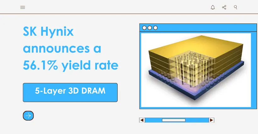
SK Hynix presented a research paper on 3D DRAM at the global semiconductor conference “VLSI 2024” held in Hawaii from the 16th to the 20th (local time).
SK Hynix reported a manufacturing yield of 56.1% for 5-layer 3D DRAM.
When approximately 1,000 3D DRAMs are manufactured on a test wafer, about 561 qualify as acceptable products.
The data shows that experimental 3D DRAM exhibits characteristics similar to those of the currently widespread 2D DRAM.
Although SK Hynix had previously mentioned the development of 3D DRAM, this is the first time specific numbers and operational characteristics have been disclosed.
Industry evaluations of this paper indicate that SK Hynix is getting closer to securing the original technology for next-generation DRAM.
3D DRAM is gaining attention as a next-generation memory product.
Conventional DRAM arranges storage elements on a flat surface, while 3D DRAM stacks these elements vertically, like an apartment building.
While its advantage is the ability to place more storage elements in the same space, it faces challenges in technical implementation.
This also means that once the core technology is secured, the DRAM paradigm can change.
SK Hynix’s competitors, such as Samsung Electronics and Micron Technology, are also developing 3D DRAM.
In particular, Samsung Electronics expressed its ambition for future technological leadership at the “Memcon 2024” exhibition in the U.S. this March, stating that it plans to mass-produce the product by 2030.
At this conference, SK Hynix indirectly countered Samsung, revealing its determination to innovate in the 3D DRAM market, similar to its advancements in the HBM field.
An insider indicated that integrating storage elements and peripheral circuits in 3D DRAM is challenging, but achieving normal operation after this process is a significant breakthrough, making SK Hynix the first company to solve this issue. Competitors have yet to overcome this problem, which SK Hynix has already managed to address.
However, while SK Hynix sees the potential of 3D DRAM, it also acknowledges that many development processes are needed for commercialization.
Unlike existing 2D DRAM, it exhibits unstable operational characteristics, and for general purposes, the paper suggests that the storage elements need to be stacked in layers ranging from 32 to 192.
Source: IEEE
Related:
- Why Edge AI Systems Rely on SRAM Compute in Memory
- Kioxia Unveils Three New Storage Technologies at IEDM 2024
- First DRAM-Free NVMe SSD Breaks New Ground in Storage

Disclaimer: This article is created by the original author. The content of the article represents their personal opinions. Our reposting is for sharing and discussion purposes only and does not imply our endorsement or agreement. If you have any objections, please get in touch with us through the provided channels.


