According to a report by South Korean media outlet The Elec on May 7th, SK Hynix is sending test wafers to Tokyo Electron (TEL) to evaluate its low-temperature etching equipment, which could be adopted in future NAND flash production.
Currently, increasing the number of stacked layers is the primary method to enhance the capacity of individual 3D NAND flash chips. However, as the number of layers increases, etching vertical channels in the chips becomes increasingly challenging due to the rising aspect ratio, which also slows down the process.
Manufacturers have to consider splitting the overall NAND flash into multiple stacks for production and then bonding them together. However, multi-stack structures introduce new issues like alignment during bonding, and performance and energy efficiency may suffer.
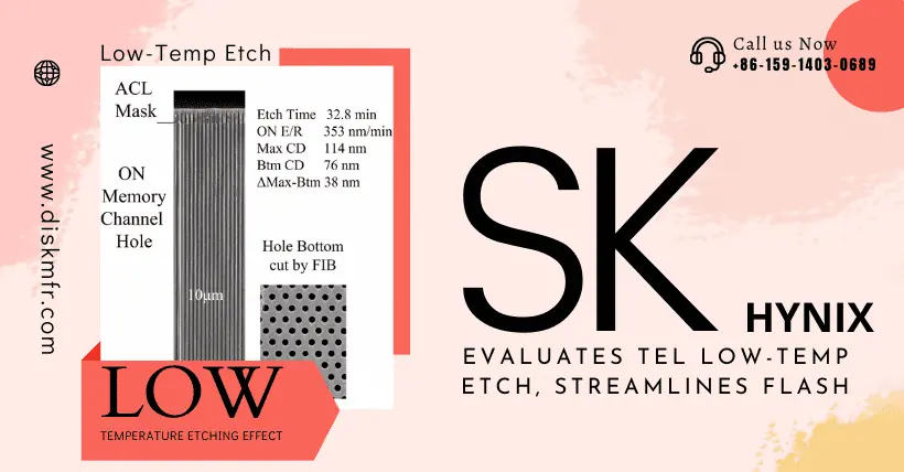
Tokyo Electron’s new low-temperature etching equipment operates at -70°C, significantly lower than the 0-30°C range of existing equipment.
According to a report by DiskMFR last year, the new equipment can etch 10 micrometers in 33 minutes, over three times faster than existing equipment.
Additionally, Tokyo Electron’s low-temperature etching equipment uses hydrogen fluoride (HF) gas, which is more environmentally friendly than the fluorocarbon gases used in traditional systems due to a lower greenhouse effect.
SK Hynix’s latest 321-layer NAND flash, announced officially, uses a three-stack structure. Industry experts anticipate that if Tokyo Electron’s low-temperature etching equipment proves effective, future 400+ layer flash products could potentially reduce the number of stacks to two or even one.
Meanwhile, one of SK Hynix’s main competitors, Samsung Electronics, is evaluating a demonstration version of the tool to assess the low-temperature etching.
Related:
- Chip Fabrication: Key Semiconductor Processes Overview
- 100 Tips of Essential Knowledge for Chip Manufacturing Pros
- Android 16 Cloud Build: Faster Software Installation
- Full Chip Manufacturing Process: From Beginner to Expert

Disclaimer: This article is created by the original author. The content of the article represents their personal opinions. Our reposting is for sharing and discussion purposes only and does not imply our endorsement or agreement. If you have any objections, please contact us through the provided channels.


