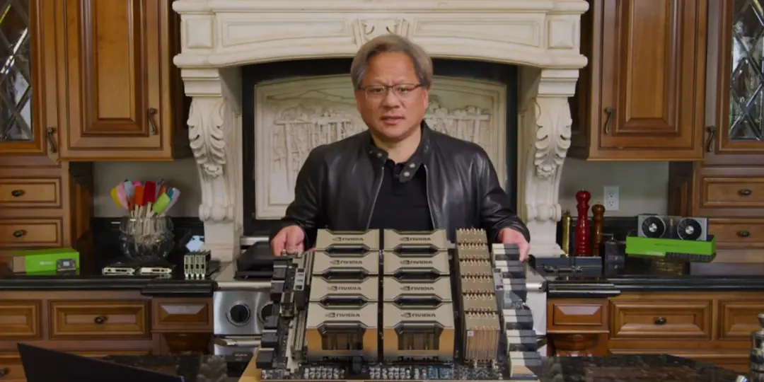
Over the past year, tech companies around the world have been scrambling to purchase AI chips, leading to a supply that cannot meet demand.
Nvidia’s production capacity has been severely limited, largely due to a shortage of HBM (High Bandwidth Memory). Each H100 chip requires 6 pieces of HBM. Currently, SK Hynix and Samsung supply 90% of the HBM, and their technology is an entire generation ahead of Micron.
This has given the Koreans an unprecedented opportunity.

It is well known that the memory market has always maintained a tripartite situation. Among them, the Koreans dominate: Samsung and SK Hynix together occupy seventy percent of the market. But Micron, ranked third, still holds more than 20% of the market share. The competition between them is fierce, with each having their victories and defeats.
The Koreans are likely dissatisfied with this situation. In the 1980s, Japan once captured more than 90% of the memory market; this overwhelming monopoly was the ultimate dream of the Korean semiconductor industry.
Therefore, at the beginning of 2024, the South Korean government designated HBM as a national strategic technology and provided tax incentives to HBM suppliers, preparing to charge forward once again.
Now, it seems that the Koreans are only one step away from turning their dream into reality.
01
Von Neumann’s “Trap”
The Koreans owe their latest opportunity largely to the “father of the computer,” John von Neumann.
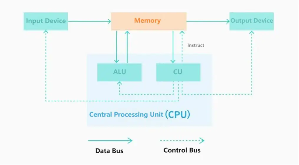
In 1945, just as the world’s first computer, ENIAC, was about to be introduced, von Neumann and his colleagues published a paper outlining a new computer architecture. The biggest breakthrough was the “separation of storage and computation” — this was the first time the logic unit was separated from the storage unit.
If you imagine the inside of a computer as a kitchen, then the storage is like the pantry manager, while the logic chip is the chef.
Initially, both “cooking” and “pantry management” were done by the same chip; it was only after the concept of “separation of storage and computation” was introduced that computers began to establish multiple “positions” and “recruit talent” for each.
The separated logic chip eventually evolved into today’s CPUs and GPUs.
The benefits of this are obvious: with storage and logic chips each specializing in their tasks, operations are as smooth as an assembly line, efficient and flexible, quickly gaining the favor of the first generation of computer designers and continuing to this day, enduringly popular.
This is the now-famous von Neumann architecture.
However, the “father of the computer,” von Neumann, unintentionally planted a “bomb” when designing this architecture.
For the von Neumann architecture to be maximized in efficiency, there is an implicit premise:
The speed of data transfer from the storage to the logic chip must be greater than or equal to the computational speed of the logic chip. In layman’s terms, the speed at which the pantry manager delivers ingredients to the kitchen must be faster than the chef’s cooking speed.
However, the reality of technological development took the opposite path.
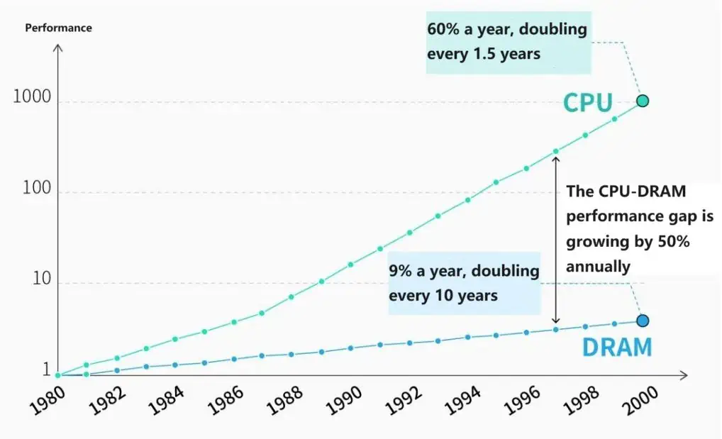
Storage clearly could not keep up with the pace of logic chip iteration. Taking CPUs as an example, the imbalance in performance was undeniable as early as the 1980s. By the turn of the 21st century, the performance gap between CPUs and storage was growing at a rate of 50% per year.
This led to a situation where the computational power limit of a chip was not determined by the logic chip’s computational power but by the memory’s transfer speed. The chef has significantly outpaced the pantry manager, and how many ingredients the manager can deliver decides how many dishes can be prepared.
This is what’s commonly referred to as the “memory wall,” the trap left by von Neumann.
In the last century, some attempted to change the status quo, and a batch of new chip architectures emerged. However, it was difficult to challenge the established, especially compared to the benefits brought by the ecosystem built around the von Neumann architecture — including programming languages, development tools, operating systems, etc., the slight performance improvements were negligible.
That was until the surge of artificial intelligence.
02
A New Spark
Artificial intelligence, based on deep learning, has an almost pathological demand for computational power.
OpenAI once made an estimation: from the 2012 AlexNet model to Google’s AlphaGo Zero in 2017, computational power consumption increased by a whopping 300,000 times. With the advent of the Transformer, “great strength brings miracles” has become the underlying logic of the AI industry, with almost all tech companies struggling with insufficient computational power.
As the “chief culprit” hindering the progress of computational power, the von Neumann architecture was quickly pushed into the spotlight.
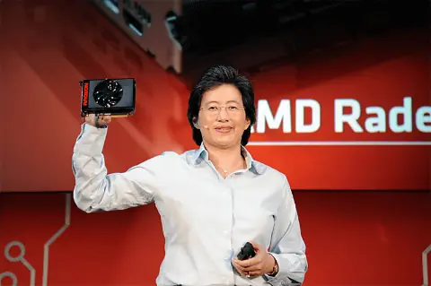
AMD was one of the first tech giants to realize the severity of the problem. It adopted a very “simple and crude” solution—placing the memory closer to the logic chip. If I build the “warehouse” closer to the “kitchen,” wouldn’t the delivery speed increase?
However, at that time, AMD’s solution had a fatal flaw.
In the past, memory was usually mounted outside the GPU package through slots, equivalent to building a warehouse in the suburbs.
However, to shorten the distance, AMD planned to move the memory to the same substrate within the same package as the GPU. However, the substrate area is very limited, like the highly valuable central urban area. Traditional memory often occupies a large area, like a huge warehouse, which obviously cannot be built in the central urban area.
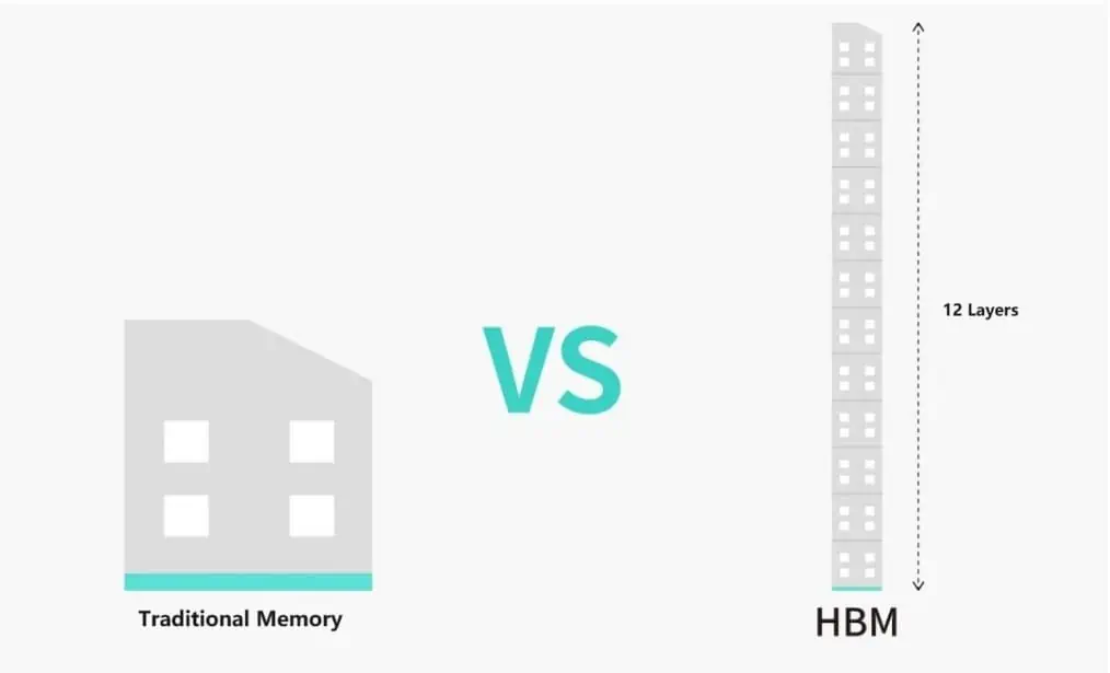
At this point, HBM began to take the stage: it utilized a method of vertically stacking small DRAM dies.
We can imagine HBM as a 12-story ultra-mini warehouse. Because the warehouse occupies a small area, the demand for land significantly decreases, allowing it to naturally move into the central urban area; at the same time, from the 1st to the 12th floor, each level can store data, so the actual performance does not decrease.
Currently, the surface area of HBM is only 6% of that of traditional memory. This new technology allowed AMD’s technical solution to be successfully implemented.
Thus, AMD extended an olive branch to SK Hynix across the Pacific.
In 2015, AMD launched the GPU Fiji, arranging 4 HBM chips on a single chip substrate, causing a small shock within the industry. The high-end graphics card Radeon R9 Fury X, equipped with Fiji, surpassed Nvidia’s Kepler series in terms of paper computational power for the first time that year.
Although Fiji was a market failure in hindsight, it did not prevent HBM from making a stunning appearance and stirring up the waters.
03
A Game for the Few
As global tech companies begin to bet on artificial intelligence, breaking through the “memory wall” with HBM, it too has taken center stage in this era.
However, only a few can share the cake from the HBM wave. Currently, as HBM is about to enter its fourth generation, the table has always been missing a fourth player. As of 2023, only three manufacturers can produce HBM: SK Hynix, Samsung, and Micron. Unfortunately, this situation is likely to persist for a long time.
Although the three giants also monopolize traditional memory, in times of market prosperity, second and third-tier manufacturers can enjoy the benefits. But in the HBM field, other manufacturers can’t even get a seat at the table, let alone share the soup.
The high technical threshold is an important reason for this situation.
As mentioned earlier, HBM is like a high-rise mini-warehouse; the design of such high-rise structures is a significant challenge.
The technology currently used in the industry is called TSV (Through-Silicon Via), which is the only vertical electrical interconnect technology available. Through etching and plating, TSV passes through the stacked DRAM dies, enabling communication between layers, akin to installing elevators in a building.
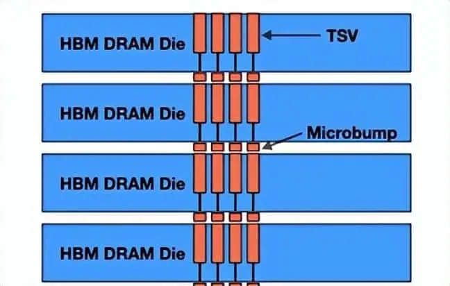
Due to the extremely small area of HBM, the requirements for the precision of the TSV process are extremely stringent. The difficulty of this operation is comparable to drilling a hole in a grain of rice. Moreover, HBM requires more than “drilling a hole”: as the building gets taller, the demand for TSVs correspondingly increases.
The three giants have the deepest accumulation of TSV technology, enough to easily leave behind other small factories and secure their position at the top.
Another reason is that HBM breaks the traditional memory IDM model, requiring external support, making it so that they cannot have the final say.
The IDM model refers to the memory manufacturer handling everything from design and manufacturing to packaging. In the past, memory manufacturers like Samsung were able to wage price wars because they controlled the entire manufacturing process, allowing them to squeeze profit margins to the maximum.
However, with HBM, while design and manufacturing are still in-house, packaging must rely on foundries.
HBM is not an independent memory module and needs to be installed next to the logic chip. This process involves more delicate operations, more precise equipment, and more expensive materials, necessitating the use of advanced packaging technologies. Currently, only TSMC’s advanced packaging technology meets the standards, and the three giants are its customers.
TSMC’s advanced packaging technology, CoWoS, has quite limited capacity, not enough to satisfy the demands of the three giants; new players looking to enter the game must rely on TSMC’s willingness to include them.
The high technical barrier and dependency on TSMC’s advanced packaging capacity mean HBM will likely remain a game for the few. These characteristics ensure that the strategy of the HBM war is fundamentally different from memory wars.
04
Reshaping the Game Rules
Traditionally, competition in the memory sector often revolves around price wars because traditional memory is a highly standardized product with little performance difference between manufacturers. Usually, the one offering the lower price gets more orders.
However, for HBM, the side with faster technological iteration holds the initiative.
Since HBM is mainly used in AI chips, its main selling point is performance. A powerful AI chip can significantly shorten the time to train models. For tech companies, spending more to get big models to market sooner is worth the extra cost.
Therefore, in the past few years, memory manufacturers have been intensely focusing on technological innovation.
Samsung managed to overtake SK Hynix in the HBM market in 2016 precisely because it was the first to mass-produce the new generation of HBM 2, taking a technological lead.
On the other hand, allying with a strong partner is equally important.
The world has only a handful of companies capable of producing AI chips, making reliance on major customers very high. Over the past few years, the competition among SK Hynix, Samsung, and Micron over HBM has essentially been about who can secure stronger alliances.
SK Hynix was the first to enter the market, partnering with the ambitious AMD. Unfortunately, AMD’s chip sales were disappointing, affecting the demand for SK Hynix’s HBM.
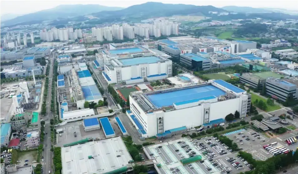
In contrast, Samsung was quite “cunning,” using its first-to-market HBM2 to successfully partner with Nvidia, overtaking SK Hynix.
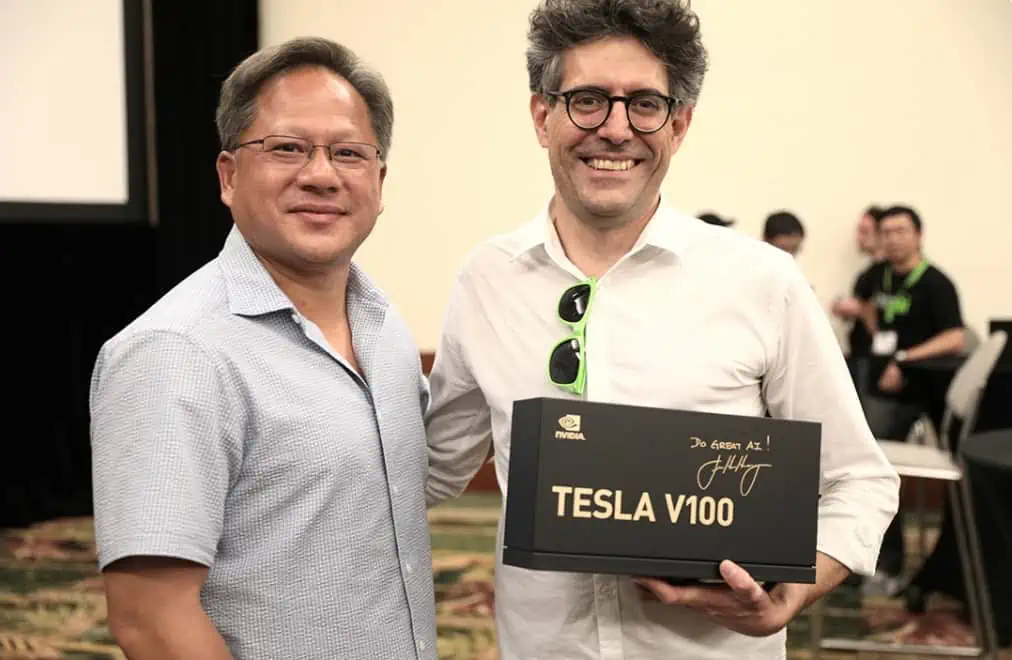
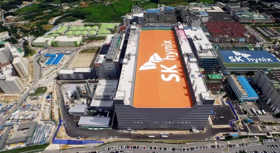
However, in 2021, SK Hynix was the first to mass-produce HBM 3, successfully drawing Nvidia to its side. The globally sought-after AI chip H100 uses HBM from SK Hynix. With this new partnership, SK Hynix firmly established itself as the leading HBM supplier.
Compared to the Korean companies, Micron had the worst luck, teaming up with Intel.
In 2016, Micron and Intel bet on a different technological path. After years of dedicated research, Micron realized it had chosen the wrong direction. By then, Micron was already two generations behind its Korean competitors.
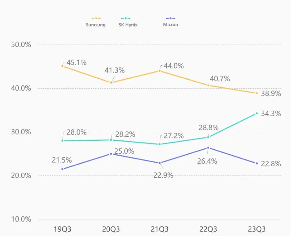
Currently, SK Hynix holds about 50% of the overall HBM supply, with Samsung capturing 40%, and Micron only 10%.
Driven by its HBM business, SK Hynix’s market share in the memory sector surged to 34.3% in the last quarter, nearly surpassing Samsung, which has been the top memory market leader for over 30 years.
However, competing in innovation speed and alliances introduces greater unpredictability. Although the three manufacturers currently seem to rank first, second, and third, each has its strengths, slowly revealing the tip of the iceberg.
05
The Trump Cards of the Three Giants
As the inventor of HBM and currently, in first place, SK Hynix’s biggest trump card is its leading technological prowess.
To completely dominate the competition, SK Hynix plans to revolutionize HBM’s design philosophy. It aims to mass-produce HBM 4 by 2026, planning to place HBM directly on top of the GPU, moving towards a true 3D architecture. In other words, SK Hynix plans to build the “warehouse” right above the “kitchen.”
At first glance, the design philosophy of HBM 4 might not seem astonishing.
After all, the original intent of HBM’s design was to shorten the distance between the “warehouse” and the “kitchen”; moving the warehouse directly above the kitchen seems like a natural choice. However, the reality is not so simple.

Previously, the reason why major memory manufacturers did not adopt this design was due to unresolved cooling issues:
Placing HBM on top of the GPU indeed speeds up data transfer, but it also significantly increases chip power consumption, generating more heat. If the heat cannot be dissipated in time, it will greatly reduce the chip’s efficiency and cause performance loss, a situation akin to robbing Peter to pay Paul.
Therefore, to realize the design of HBM 4, a better cooling solution must be found.
Currently, SK Hynix may have found a breakthrough; if successfully implemented, it would undoubtedly be a dimensional strike against competitors.
However, SK Hynix’s model has a flaw—too much reliance on TSMC.
As mentioned earlier, HBM technology is highly tied to TSMC’s advanced packaging. But currently, TSMC’s capacity is far from meeting market demand, leaving room for Samsung to potentially overtake the curve.
Samsung is not only the biggest player in the memory market but also the world’s second-largest foundry. TSMC has advanced packaging capabilities, and so does Samsung, albeit at a slightly lower level.
As early as 2018, Samsung introduced its I-Cube technology, which competes with TSMC’s, and by 2021 it had developed to the fourth generation.
Currently, Samsung’s I-Cube technology is not as good as TSMC’s CoWoS, after all, even Samsung itself doesn’t use it. But with TSMC’s capacity unable to meet demand, I-Cube technology has become Samsung’s weapon to attract business.
SK Hynix’s old partner AMD was unable to resist the “temptation of capacity” and changed camps. Nvidia is also rumored to be interested in testing the waters, as TSMC’s limited increase in advanced packaging production means utilizing Samsung helps diversify supply risks.
What countermeasures do the Americans have?
To be honest, up to this point, Micron has been in a passive and never-turning situation on the HBM battlefield. After years of catching up, Micron has finally seen the backs of the leaders but can only follow behind the Koreans “picking up leftovers.”
The ultimate dream of the Koreans to “unify the memory empire” seems to be just one step away.
However, this is not what the Americans would like to see. Currently, most of HBM’s major customers are from the United States. Although Micron is behind, it is not necessarily completely out of the game. Recent leaks show that Nvidia has just placed an order for HBM 3 with Micron.
Previously, the Koreans were able to “win every battle” in the memory market because the rules of competition were very clear: it was all about capacity and cost. Internal competition has always been the “comfort zone” for Koreans, as their veins run with American coffee.
However, HBM is not a “typical East Asian” industry. It faces extremely harsh technical competition and ever-fluctuating major customers. The increased unpredictability prevents the Koreans from securely holding the iron throne. Moreover, another mysterious force from the East is also eyeing eagerly.
The long night is far from over, and the Koreans still cannot rest easy.

Disclaimer: This article is created by the original author. The content of the article represents their personal opinions. Our reposting is for sharing and discussion purposes only and does not imply our endorsement or agreement. If you have any objections, please contact us through the provided channels.


