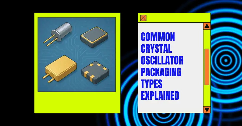
Common Crystal Oscillator Packaging Types Explained
Explore common crystal oscillator packaging methods and their features, enhancing reliability, precision, and efficiency in electronic applications.

Explore common crystal oscillator packaging methods and their features, enhancing reliability, precision, and efficiency in electronic applications.
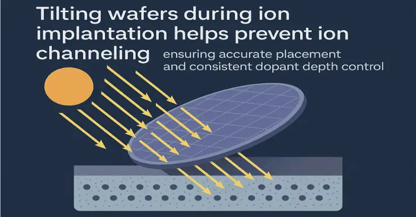
Tilting wafers during ion implantation helps prevent ion channeling, ensuring accurate placement and consistent dopant depth control.
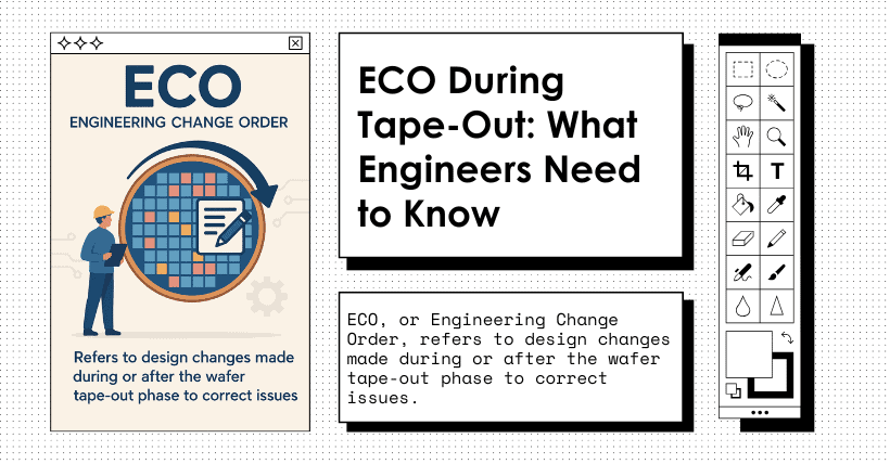
ECO, or Engineering Change Order, refers to design changes made during or after the wafer tape-out phase to correct issues.

Gaming test reveals if Ryzen 5 5600 bottlenecks GeForce RTX 5060—see real performance insights and smooth gameplay results.
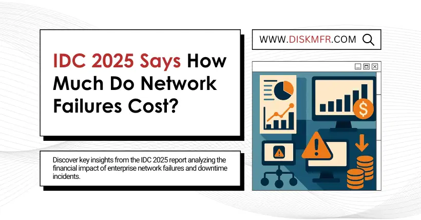
Discover key insights from the IDC 2025 report analyzing the financial impact of enterprise network failures and downtime incidents.
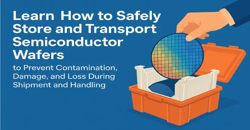
Learn how to safely store and transport semiconductor wafers to prevent contamination, damage, and loss during shipment and handling.
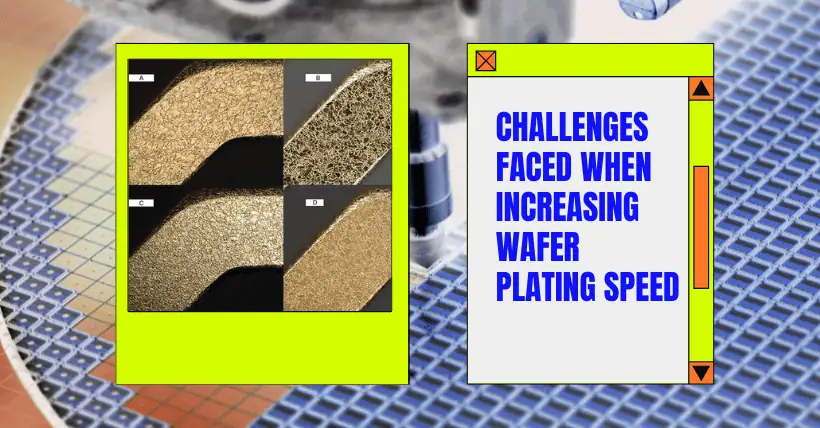
The wafer electroplating rate cannot be increased indefinitely because semiconductor processes generally follow the principle of “more haste, less speed.”

Testing gold bump hardness post-annealing ensures structural integrity, bonding strength, and long-term performance in microelectronic applications.
