
Scanning Acoustic Microscopy (SAM) has become indispensable testing equipment for semiconductor supply chain integrity, online manufacturing, research and development, and quality control laboratories. It can even perform a comprehensive 100% inspection of all manufacturing materials.
Manufacturers’ testing laboratories, research centers, material research groups, and quality control departments are seeking investments in SAM equipment due to the need for detecting tiny defects. Failure analysis and reliability testing measurement techniques have become crucial, and SAM now competes with other laboratory testing and measuring instruments such as X-rays and scanning electron microscopes (SEM). In the current highly restricted market conditions of the electronic component supply chain, SAM is a highly efficient tool that can help reduce the spread of counterfeit components in the semiconductor supply chain.
Manufacturers’ testing laboratories, research centers, material research groups, and quality control departments are increasing their investments in Scanning Acoustic Microscopy (SAM) equipment due to the need for detecting tiny defects. Failure analysis and reliability testing measurement techniques have become crucial, and SAM is now competing with other laboratory testing and measuring instruments such as X-rays and scanning electron microscopes (SEM). In the current highly restricted market conditions of the electronic component supply chain, SAM is a highly efficient tool that can help reduce the spread of counterfeit components in the semiconductor supply chain.
SAM, also known as Non-Destructive Testing (NDT) using ultrasonic waves, is used in industry to identify small defects in products or components during the manufacturing process. It is also used to analyze the specific root cause of failures when devices fail in the field. The demand for this powerful failure detection capability is driving its increasing use among consumer, industrial, and military electronic device manufacturers.
SAM provides powerful non-invasive and non-destructive imaging and material analysis to inspect the internal structure of opaque materials. It can extract information at specific depths and apply it to create two-dimensional and three-dimensional images, without the need for time-consuming tomography scans or expensive X-ray equipment. Experts can analyze SAM images to detect and characterize device defects such as cracks, delaminations, inclusions, and voids in bond interfaces, as well as evaluate soldering and other interface connections on PCBs.
The latest advancements in SAM have enabled the detection of much smaller defects than before.
“Advanced phased array SAM systems are raising the bar for failure analysis, as they improve the level and accuracy of detection. The previous goal was to detect defects of 500 microns; now the target has become detecting defects of 50 microns. Through this type of testing, we can examine materials and discover defects that were previously undetected,” said Hari Polu, President of OKOS, an industrial SAM NDT system manufacturer based in Virginia that serves the markets of electronic manufacturing, aerospace, and metal/alloy/composite material manufacturing as well as end-users.
As manufacturers use higher-level failure detection and analysis tools, production yield and overall reliability of electronic devices significantly improve. This results in faster project completion and potential failure points on site can also be eliminated.
Due to the significant advantages of using SAM, more and more manufacturers are equipping their R&D and QA laboratories with SAM measurement equipment and integrating it into their production lines for 100% full inspection.
① SAM meets the needs of the semiconductor and electronic components industry
The demand for non-destructive failure analysis and reliability testing is rapidly increasing in the semiconductor and electronic component industries. Consistency and absence of defects or impurities are crucial in manufacturing in these industries. Whether it’s wafer-level components, discrete electronic components, or packaging components used in smartphones, video games, EV car subsystems, or rocket subsystems, the situation is the same.
SAM meets this need in the semiconductor and electronic component industries. This testing has become the industry standard for 100% testing of semiconductor components, used to identify defects such as gaps, cracks, and delamination of different layers in microelectronic devices.
In addition to semiconductor components themselves, today’s electronic component products also include various specialty metal, alloy, plastic, and glass components. All semiconductor components need to be integrated and packaged in a form that is available to consumers. Therefore, SAM equipment has developed synchronously, now being used to detect defects, delamination, cracks, and other irregularities beneath the surfaces of these types of materials that make up the “packaging” of semiconductor components.
Due to the critical properties of many components made with these materials, high-purity alloys should be highly consistent, with low levels of impurities and contaminants. High-purity metals and alloys such as aluminum, zinc, cobalt, copper, titanium, zirconium, molybdenum, magnesium, and stainless steel are the backbones of many industries such as electronic components, aerospace, and medical devices.
② SAM equipment saves costs and time
The function of a scanning acoustic microscope (SAM) is to focus sound waves from a transducer onto a small point on a target object. The sound waves that hit the object are scattered, absorbed, reflected, or transmitted. By detecting the direction and “flight time” of the scattered pulses, the presence and distance of boundaries or objects can be determined.
To generate an image, the sample is scanned point-by-point or line-by-line. Scanning modes range from single-layer views to tray scanning and cross-sections. Multilayer scans can include up to 50 independent layers. Specific depth information can be extracted and applied to create 2D and 3D images without the need for time-consuming tomographic scan procedures or expensive X-ray equipment. The images can then be analyzed to detect and characterize defects such as cracks, inclusions, and voids.
As demand increases, manufacturers typically use larger systems with high-speed detection capabilities to accommodate testing in higher volume production. However, the challenge then becomes to execute such inspections at extremely high throughput and to identify and remove components that do not meet quality requirements through 100% inspection. This requires more advanced equipment that can examine multiple layers simultaneously and is typically automated to scan and process multiple samples in trays across multiple channels to expedite the process.
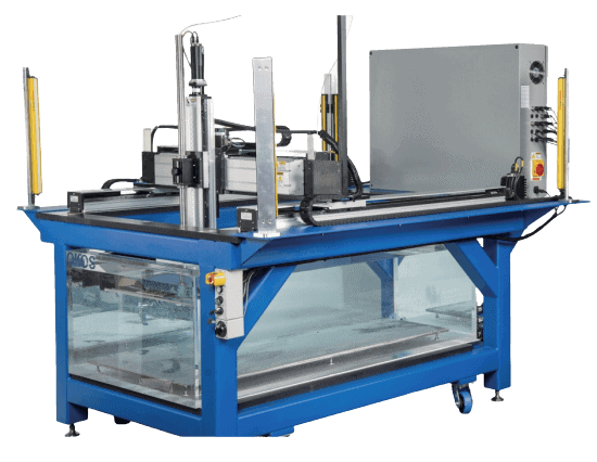
Smaller manufacturers and independent testing labs can opt for a desktop SAM, which offers a scan range of over 300mm, a maximum scan speed of 500mm/s, and accuracy and repeatability of +/-5.0μm. Its software allows for virtual rescanning, viewing, and analysis of saved data for synchronous real-time analysis or post-collection review. Typically, such desktop devices are used to analyze data for failure analysis, product inspection, quality control, R&D, process validation, and determining product reliability, process quality control, and supplier qualification.
As demands increase, manufacturers typically use larger systems with high-speed detection capabilities to adapt to testing in high-level production. However, the challenge here is to perform this inspection at extremely high throughput rates and to identify and remove components that do not meet quality requirements through 100% inspection. This requires more advanced equipment that can simultaneously inspect multiple layers, usually in multiple channels, and automatically scan multiple samples in processing trays to speed up the process.
According to Polu, SAM can also be custom designed for full integration into high-volume manufacturing systems. Advanced phased array systems can detect small defects in specialty metals and alloys, enabling 100% inspection of all materials. Semiconductor factories can now perform 100% inspection of wafers, panels, and separated components in trays.
Fortunately, recent advancements in SAM technology have significantly improved throughput and defect detection capabilities. When 100% inspection requires high throughput, ultra-fast single or double gantry scanning systems with 128 sensors for phased array scanning can be used. Multiple transducers can also be used to scan simultaneously for even higher throughput.
“Traditional 5MHz sensors may take up to 45 minutes to inspect an 8-10 inch square or circular alloy. However, the advanced phased array with 64-128 sensors and innovative software for rendering images can reduce inspection time to five minutes and detect small impurities or defects more precisely,” says Polu.
In addition to the physical and mechanical aspects of hardware used for scanning, the software is equally important for improving resolution and analyzing information to generate detailed scans.
Multi-axis scanning options support A, B, and C scanning, contour tracking, offline analysis, and virtual rescanning of composite materials, metals, and alloys. Inspection software can perform high-precision internal and external inspections of defects and thickness measurements.
Various software modes can achieve simplicity and ease of use, detailed analysis, and automated production scanning. The offline analysis mode can also be used for virtual scanning.
Polu estimates that OKOS’s software-driven model enables them to lower the cost of SAM testing while still providing the same quality inspection results. Therefore, even general testing laboratories can use this type of equipment.
“Due to today’s strict requirements for detection and accuracy, every company will eventually turn to higher levels of failure analysis,” said Polu. “The cost advantage and time savings of industrial SAM equipment make this requirement possible.”
OKOS has laboratories in Santa Clara, California, Phoenix, Arizona, and Manassas, Virginia, providing contract analysis and testing services that comply with existing industrial and military standards. This service also allows customers to review technology and feasibility before investing in equipment.
Today, in many industries, compared to traditional methods, the level of failure analysis detail provided by SAM is extremely high, making it the best value. Therefore, advanced SAM systems are now widely regarded as essential tools in R&D and quality assurance laboratories, as well as high-speed production lines.
Related:

Disclaimer: This article is created by the original author. The content of the article represents their personal opinions. Our reposting is for sharing and discussion purposes only and does not imply our endorsement or agreement. If you have any objections, please contact us through the provided channels.


