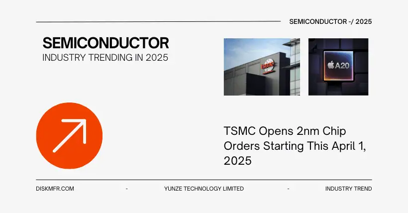
Starting April 1, TSMC will officially open order channels for its 2nm wafer process. TSMC Chairman Mark Liu revealed that customer demand for 2nm technology has even exceeded that of 3nm at the same stage. Apple is expected to secure the first batch of supply, and according to the latest analysis from renowned Apple supply chain analyst Ming-Chi Kuo, the entire iPhone 18 series, scheduled for release in the second half of 2026, will be equipped with the A20 processor, potentially making it the world’s first to adopt the 2nm process.
The A19 chip in the iPhone 17 series will be manufactured using TSMC’s third-generation 3nm process (N3P). If the A20 chip enters mass production as planned, it will see significant improvements in performance and energy efficiency. Industry analysts suggest that the A20’s performance boost could surpass previous generations, while also enabling Apple to explore new designs such as foldable screens and under-display Face ID.
Ming-Chi Kuo also mentioned on social media that the risk trial yield rate for TSMC’s 2nm process reached 60% to 70% three months ago and has since improved. TSMC is currently ramping up 2nm capacity, with its factories in Kaohsiung and Baoshan, Hsinchu, playing key roles. The Kaohsiung plant will hold a 2nm capacity expansion ceremony on March 31 before accepting orders, with the first batch of wafers expected to arrive in Baoshan by the end of April.
In addition, a number of major clients—including AMD, Intel, Broadcom, and AWS—are lining up for 2nm capacity. A research report by Morgan Stanley states that in 2025, TSMC’s monthly 2nm production capacity will increase from a pilot scale of 10,000 wafers to around 50,000 for mass production. With the full launch of the Kaohsiung and Baoshan plants, monthly capacity is expected to expand to 80,000 wafers.
At the IEDM 2024 conference, TSMC disclosed technical details of its 2nm process for the first time. The 2nm process uses gate-all-around (GAA) nanosheet transistor technology. Compared to the previous generation 3nm process, transistor density increases by 15%, performance improves by 15% at the same voltage, and power consumption is reduced by 24% to 35% at the same performance level. The process is optimized through the N2 NanoFlex design technology, allowing for smaller, more energy-efficient logic units. It also supports six voltage threshold levels spanning a 200mV range, offering greater design flexibility.
TSMC’s 2nm process achieves an SRAM density of 38Mb/mm², a significant improvement over previous generations. Wire resistance has been reduced by 20%, and paired with ultra-high-performance MiM capacitors, the process provides stronger support for high-frequency computing scenarios. These technological breakthroughs have led to widespread industry optimism about the application potential of 2nm chips in AI and high-performance computing (HPC).
It is worth noting that the cost per 2nm wafer is about $30,000. TSMC hopes to attract more customers by further reducing costs, and may launch a “CyberShuttle” service in April to help clients cut expenses—allowing them to evaluate chips on the same test wafer and reduce R&D costs. TSMC has already achieved near-monopoly in the global 3nm chip competition, and the latest updates suggest its lead in 2nm technology is even more dominant—Samsung has yet to attract enough customers for its 2nm chip foundry services, and Intel lags behind in technology.

Disclaimer:
- This channel does not make any representations or warranties regarding the availability, accuracy, timeliness, effectiveness, or completeness of any information posted. It hereby disclaims any liability or consequences arising from the use of the information.
- This channel is non-commercial and non-profit. The re-posted content does not signify endorsement of its views or responsibility for its authenticity. It does not intend to constitute any other guidance. This channel is not liable for any inaccuracies or errors in the re-posted or published information, directly or indirectly.
- Some data, materials, text, images, etc., used in this channel are sourced from the internet, and all reposts are duly credited to their sources. If you discover any work that infringes on your intellectual property rights or personal legal interests, please contact us, and we will promptly modify or remove it.


