Taiwan Semiconductor Manufacturing Company (TSMC) is a joint venture established on February 21, 1987, between the Taiwan, Philips, and other private investors. TSMC is currently the world’s largest wafer foundry in the semiconductor industry. TSMC manufactures semiconductors based on proprietary integrated circuit designs from customers or third parties, using its manufacturing processes. TSMC offers comprehensive wafer manufacturing processes, including the production of CMOS logic, mixed-signal, RF, embedded memory, BiCMOS mixed-signal, and other semiconductor processes. TSMC also provides design, mask-making, probing, testing, and assembly services.
Company Address: No. 8, Lixing 6th Road, Hsinchu Science Park, Taiwan.
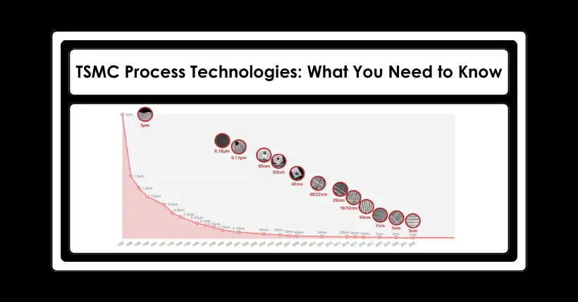
I. TSMC Process Technology Overview (by Node Evolution)
✅ 0.18μm ~ 0.13μm ~ 90nm
0.18μm (1998): The world’s first low-power process. This greatly facilitated the development of mobile communications and portable electronic devices.
0.13μm (2002): The world’s first low-k dielectric and copper interconnect integrated SoC process, breaking the performance and power consumption bottleneck.
90nm (2004): The world’s first 193nm immersion lithography application in mass production, with significant improvements in transistor density and performance.
Applications: Mobile phones, laptops, consumer electronics, first-generation smart devices.
✅ 65nm ~ 55nm
65nm (2005): The first mass-produced low-power (LP) process, introducing multiple derivative processes such as GP, MS/RF.
55nm: A simplified, optimized version of 65nm, with smaller dimensions and further reduced power consumption, suitable for IoT and automotive markets.
Features: Double the cell density of 90nm, significant improvement in energy efficiency. Applications: Smartphones, IoT devices, automotive chips, wearables.
✅ 40nm
40nm (2008): The first use of 193nm immersion lithography combined with ultra-low k materials, enhancing performance and reducing power consumption.
40LP / 40ULP: Specially adapted for smartphones, digital TVs, wearable devices, and low-power IoT products.
Features: The industry’s smallest SRAM size at the time (0.242µm²). Extension technologies: RF, embedded flash, BCD processes.
✅ 28nm ~ 22nm
28nm (2011): TSMC launched the most comprehensive 28nm process family (including 28HPC/28HPC+/28ULP, etc.).
22ULP / 22ULL (2018): Further reduced power consumption based on the 28nm process, targeting low-power applications such as wearables and IoT.
Applications: 5G RF, automotive radar, IoT SoC, battery-powered consumer products.
✅ 20nm
20nm (2014): The world’s first mass production process using double patterning.
Special emphasis on transistor and interconnect energy efficiency, suitable for high-performance computing and high-density integrated chips.
Milestone: TSMC’s fastest ramp-up to mass production.
✅ 16/12nm FinFET
16nm FinFET (2015): TSMC introduced FinFET 3D transistor architecture, significantly reducing leakage current and improving performance.
12nm: A performance-enhanced version of 16nm, improving density and power consumption.
Suitable for: High-performance computing (HPC), high-end mobile application processors (AP).
✅ 10nm
10nm (2017): A 2.1x density improvement over 16nm, with a 40% reduction in power consumption.
Applications: High-end mobile processors.
✅ 7nm (N7/N7+)
N7 (2018): A mass production node, first supporting both smartphone and HPC applications.
N7+ (2019): The first mass production node using EUV (Extreme Ultraviolet Lithography) process.
Applications: 5G chips, server CPUs, AI accelerators.
✅ 6nm (N6)
N6 (2020): An evolution of 7nm, compatible with N7 IP, improving performance and density.
Suitable for: Smartphones, high-performance computing, consumer electronics.
✅ 5nm (N5/N5P/N4/N4P/N4X/N5A)
N5 (2020): The second generation EUV node, offering optimal power, performance, and area (PPA) characteristics.
N5P / N4 / N4P: Successive optimizations, continuously improving frequency and reducing power consumption.
N4X: A version tailored for HPC.
N5A: Optimized for automotive applications.
Features: Suitable for flagship smartphones, AI/HPC accelerators, automotive-grade chips.
✅ 3nm (N3/N3E/N3P/N3X/N3AE)
N3 (2022): The final generation of FinFET architecture, further enhancing PPA advantages.
N3E / N3P: Performance-enhanced versions.
N3X: Custom designed for ultra-high-performance computing (HPC).
N3AE: Targeted at automotive applications.
Note: Lower power consumption and higher density, mainly focused on AI, servers, and automotive.
✅ 2nm (N2) — [Mass production expected: 2025]
N2: The first introduction of nanosheet transistor architecture, overcoming the traditional FinFET bottleneck.
Features:
- Ultra-low resistance RDL (Redistribution Layer) re-wiring layer.
- Ultra-high-performance MiM capacitors.
- Extreme energy efficiency and transistor density.
Mass production timeline: Expected in 2025.
Customer progress: Major customers have completed 2nm IP design and are entering the silicon validation phase.
✅ A16 (based on N2 extension)
A16™: Equipped with Super Power Rail (SPR) backside power delivery architecture.
Advantages:
- Speed improvement of 8%-10%.
- Power consumption reduction of 15%-20%.
- Chip density improvement of 7%-10%.
Especially suitable for: HPC complex signal/dense power demand chips.
✅ Summary
From 90nm planar transistors to 16nm/7nm FinFET, and finally to 2nm nanosheet, TSMC continues to drive Moore’s Law forward through architectural innovations.
TSMC not only advances process technologies but also concurrently develops supporting IP, packaging, and testing technologies to create an end-to-end technological ecosystem.
Extended reading:
- SMIC’s process technology introduction
- Chip sales from entry to practice: Successful large customer sales strategies
- Simplified understanding of semiconductor industry fundamentals (essential for beginners or career changers)
II. TSMC Specialty Process Technologies
TSMC, in addition to leading the world in advanced processes (N5, N3, N2 nodes), also possesses the most complete and powerful suite of specialty process technologies, widely used in mobile devices, automotive electronics, medical devices, wearables, and IoT fields. The specialty processes mainly include:
✅ MEMS & Sensor SoC Technology Technology content:
- In 2011, TSMC pioneered Sensor SoC technology, integrating MEMS devices and CMOS logic on a single chip, combined with wafer stacking technology.
- Process nodes range from 0.5µm to 0.11µm.
- Supports G-sensors, gyroscopes, pressure sensors, microfluidics, and bio-gene chips.
Key achievement:
- In 2018, TSMC launched the world’s first single-chip CMOS-MEMS capacitive barometer with sensitivity capable of detecting 5cm height changes, with packaging dimensions smaller than 1mm².
Future plans:
- Development of highly sensitive thin-film microphones.
- Promotion of MEMS Si-pillar TSV (silicon through-via) technology for higher integration and smaller packaging.
Engineer’s key point: MEMS processes enable the integration of sensors and logic circuits, significantly reducing size and power consumption while enhancing system performance, suitable for high-end wearables, navigation, and other scenarios.
✅ CMOS Image Sensor (CIS) Technology Technology content:
- A complete image sensor process platform from 0.5µm to 12nm.
- Supports mobile phone cameras, in-vehicle imaging, machine vision, medical imaging, security monitoring, and toy cameras.
Cutting-edge progress:
- Global shutter CIS and enhanced near-infrared (NIR) CIS for machine vision and autonomous driving.
- In 2023, TSMC helped customers launch the CIS product with the highest dynamic range (HDR), specifically strengthening ADAS (Advanced Driver Assistance Systems) and autonomous driving applications.
Engineer’s key point: TSMC leads not only in mass production but also in innovating NIR perception, HDR dynamic range, speed, and energy efficiency. Machine vision and automotive imaging demands are future priorities.
✅ Embedded Non-Volatile Memory (eNVM) Technology content:
- Includes OTP (One-time Programmable), MTP (Multi-time Programmable), Flash, MRAM, RRAM.
- eFlash platform from 0.5µm to 40nm, supporting consumer, industrial, and automotive-grade applications.
Cutting-edge progress:
- 2018 mass production of 40nm automotive-grade eFlash.
- Advancement of 28nm eFlash to meet automotive electronics and MCU needs.
- Development of 40nm embedded RRAM and 22nm embedded MRAM (validated through JEDEC high-temperature lifetime testing).
Engineer’s key point: eNVM is foundational for IoT, MCU, and automotive chips. TSMC has deep expertise in low power, high reliability, and is focusing on RRAM and MRAM as next-generation ultra-low power memory.
✅ RF / Mixed Signal (MS/RF) Technology Technology content:
- Leading mixed-signal/RF processes covering 5G, Wi-Fi 7, and IoT wireless communication.
- Platforms include 12FFC+ RF (based on N12e), N6RF/N6RF+, 16FFC RF.
Applications:
- Supports mmWave frequency bands (28/39/47GHz) and automotive radar (77/79GHz).
- Introduces NCS (Non-Conductive Stress) and aging models, optimizing automotive radar power amplifier design.
Engineer’s key point: MS/RF processes directly affect chip connectivity speed, energy efficiency, and reliability for 5G/mmWave wireless communication and smart automotive radar modules.
✅ High-Voltage (HV) Process Technology Technology content:
- From 0.5µm to 28nm, covering display driving, high-voltage analog applications.
- The 28HV process is based on the 28HPC+ platform, supporting 0.9V low Vdd, integrating 128Mb SRAM.
Applications:
- Panel driving (OLED), high-end TVs, smartphone displays, AR/VR displays (µOLEDoS).
Engineer’s key point: HV processes are crucial for OLED display driver ICs (DDIC), particularly as demand explodes for small high-PPI displays in AR/VR fields.
✅ BCD (Bipolar-CMOS-DMOS) Power Management Technology Technology content:
- Nodes range from 0.6µm to 40nm, suitable for Power Management ICs (PMICs).
- The second-generation 40nm BCD technology is compatible with ULP processes (supporting 5-28V high-voltage components).
Development direction:
- TSMC is developing the world’s most advanced 22nm BCD platform, targeting reduced power consumption, smaller chip size, and serving high-end markets like electric vehicles and servers.
Engineer’s key point: BCD technology enhances the performance and integration of power ICs, crucial for automotive-grade PMICs and mobile device power management chips.
✅ Ultra-Low Power (ULP) Technology Platform Technology content:
- Nodes include 40ULP, 22ULL, N12e, N6e.
- Supports ultra-low leakage (ULL) core devices, low Vdd SRAM, ultra-low energy logic applications.
Applications:
- IoT, wearable devices, smart homes, Industry 4.0, smart cities, AI edge computing.
Engineer’s key point: ULP technology directly determines the battery life of IoT/AIoT devices and is a core technology for enhancing chip energy efficiency in the context of energy transition and carbon neutrality.

Disclaimer:
- This channel does not make any representations or warranties regarding the availability, accuracy, timeliness, effectiveness, or completeness of any information posted. It hereby disclaims any liability or consequences arising from the use of the information.
- This channel is non-commercial and non-profit. The re-posted content does not signify endorsement of its views or responsibility for its authenticity. It does not intend to constitute any other guidance. This channel is not liable for any inaccuracies or errors in the re-posted or published information, directly or indirectly.
- Some data, materials, text, images, etc., used in this channel are sourced from the internet, and all reposts are duly credited to their sources. If you discover any work that infringes on your intellectual property rights or personal legal interests, please contact us, and we will promptly modify or remove it.


