I. Introduction
In semiconductor physics, the conduction band and the forbidden band are important concepts used to describe the energy state distribution of electrons in semiconductor materials. They form the foundation for understanding the electrical and optical properties of semiconductors as well as the working principles of semiconductor devices.
II. Definition of the Conduction Band
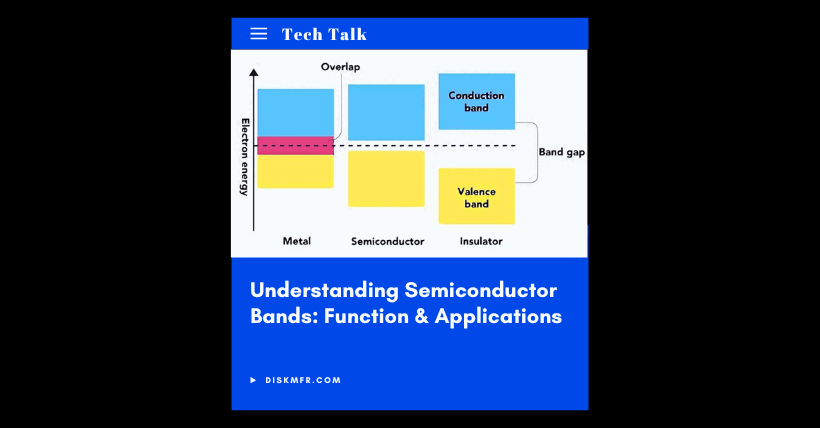
The conduction band refers to the range of energies that electrons can possess in semiconductor materials. In this energy range, electrons can move freely and participate in the conduction process. The energy of electrons in the conduction band is continuously distributed, meaning electrons can have any energy value within this range.
In semiconductors, there are typically two important conduction bands: the valence band and the conduction band. The valence band is formed by the energy levels of the valence electrons of semiconductor atoms. At absolute zero, all energy levels in the valence band are fully occupied by electrons.
The conduction band is a higher energy band than the valence band. At normal temperatures, some electrons can absorb energy and transition from the valence band to the conduction band, thus participating in conduction. Electrons in the conduction band are free electrons that can move freely in the crystal, forming an electric current.
III. Definition of the Forbidden Band
The forbidden band (or band gap) refers to the energy range in semiconductor materials where electrons are not allowed to exist, meaning there is no stable electron state in this energy range.
The forbidden band separates the valence band and the conduction band. Its width is an important physical parameter of semiconductor materials. The larger the width of the forbidden band, the more energy is required for electrons to transition from the valence band to the conduction band. The material becomes more insulating. The smaller the forbidden band width, the more the material tends to be a conductor.
IV. Interrelationship and Its Impact on Semiconductor Conductivity
✅ Interrelationship
The conduction band and forbidden band are interdependent and interconnected. The forbidden band separates different conduction bands, while the electron states and energy distribution in the conduction band are constrained by the width of the forbidden band. In semiconductors, the valence band and conduction band are separated by the forbidden band, and electrons must cross the forbidden band to transition from the valence band to the conduction band.
This transition process can occur through the absorption of photons (photo-excitation), thermal excitation, or the effect of an external electric field.
✅ Impact on Semiconductor Conductivity
The conductivity of a semiconductor mainly depends on the number of electrons in the conduction band and the number of holes in the valence band. At room temperature, due to thermal excitation, some electrons can acquire enough energy to cross the forbidden band and transition from the valence band to the conduction band, simultaneously creating a corresponding number of holes in the valence band.
Electrons in the conduction band and holes in the valence band both participate in conduction and are collectively referred to as charge carriers. The electrical conductivity of a semiconductor is related to the concentration and mobility of charge carriers. The smaller the forbidden band width, the more electrons can transition to the conduction band at the same temperature, resulting in a higher concentration of charge carriers and, consequently, a higher electrical conductivity.
V. Application of Conduction Band and Forbidden Band in Semiconductor Devices
Transistors are among the most important semiconductor devices in modern electronic technology, widely used in various circuits for amplification, switching, etc. Taking a bipolar junction transistor (BJT) as an example, it consists of three regions: the emitter, the base, and the collector, where the semiconductor types of the emitter and collector are the same, while the semiconductor type of the base is opposite to them.
During the operation of the bipolar junction transistor, the base current can be controlled to regulate the number of charge carriers injected from the emitter to the base, thus controlling the size of the collector current. This process involves complex physical processes such as the transition of electrons between the conduction band and forbidden band in different regions and the diffusion and recombination of charge carriers.
For example, in an NPN bipolar junction transistor, electrons in the emitter are injected into the valence band of the base under the forward bias of the emitter junction. Some electrons then diffuse in the base and are collected by the collector junction, forming the collector current. The width of the forbidden band and factors like the mobility of charge carriers significantly impact the current gain, frequency response, and other performance parameters of the transistor.
VI. Conclusion
In summary, the conduction band and forbidden band are crucial concepts in the field of semiconductors. They determine the fundamental physical properties of semiconductors, such as conductivity and optical properties, and play an essential role in the design, manufacturing, and application of semiconductor devices.
Related:
- WiFi 1 to 7 Compared: Key Differences Explained Today
- Exploring the Role of Charge Carriers in Electronics
- PCB Short Circuits & Pad Peeling: 80% Ignore These Tips!
- Understanding Optical Clarity in Semiconductor Films

Disclaimer:
- This channel does not make any representations or warranties regarding the availability, accuracy, timeliness, effectiveness, or completeness of any information posted. It hereby disclaims any liability or consequences arising from the use of the information.
- This channel is non-commercial and non-profit. The re-posted content does not signify endorsement of its views or responsibility for its authenticity. It does not intend to constitute any other guidance. This channel is not liable for any inaccuracies or errors in the re-posted or published information, directly or indirectly.
- Some data, materials, text, images, etc., used in this channel are sourced from the internet, and all reposts are duly credited to their sources. If you discover any work that infringes on your intellectual property rights or personal legal interests, please contact us, and we will promptly modify or remove it.


