As we enter the post-Moore’s Law era, the ability of chip manufacturers to integrate various components into a single chip is becoming increasingly important. To continue developing smaller, more densely packed, and highly integrated chips, in addition to conventional process scaling, various advanced packaging technologies are becoming indispensable. Among these, advanced packaging technologies such as flip-chip have emerged as the preferred option for packaging high-performance products. FCBGA (Flip Chip Ball Grid Array) is one such technology and has become the mainstream for flip-chip packaging.
Apple is a loyal adopter of FCBGA packaging technology. Apple was one of the earliest adopters of FCBGA packaging technology, with the A5 processor, which was used in the first generation of the iPad and iPhone 4S in 2006. Since then, Apple has been using FCBGA packaging technology and continuously improving and enhancing its performance, up to its latest PC processor, the M-series. Recently, Apple supplier LG Innotek has entered the FCBGA substrate market, leading to industry speculation that they will provide FCBGA substrates for Apple’s M-series chips. This is a testament to the growing market demand for FCBGA technology. Apple’s use of this packaging technology is currently experiencing rapid development.
① FCBGA technology is flourishing in various fields
FCBGA (Flip Chip Ball Grid Array), a packaging technology that flips the chip connects it to the packaging substrate, and then fixes the package to the substrate using spherical solder joints, is a well-established technology that first appeared in the early 1990s. In 1997, Intel Corporation first applied FCBGA packaging technology to processors, marking a significant milestone in the history of FCBGA technology. Since then, FCBGA technology has been widely adopted in various fields, including telecommunications, medical devices, automotive electronics, and consumer electronics. FCBGA packaging technology is particularly suitable for high-speed and high-density integrated circuits and is known for its excellent electrical performance, small size, and high reliability. With the continuous development and innovation of FCBGA technology, it is expected to become even more prevalent in various industries in the future.
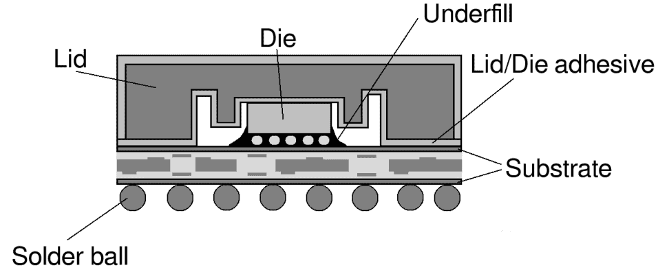
In 1999, Intel (Inside Intel Museum: Silicon Valley’s Tech Revolution) launched the first chip using FCBGA packaging technology, the Pentium III 500 processor. Before this, the main packaging method for processors was multi-chip modules (MCM), which integrated multiple chip components into one package. However, the MCM packaging method had problems such as signal interference and poor thermal management due to the complex connection lines. In contrast, FCBGA packaging technology flips the chip over and connects the metal bumps on the back of the chip to the metal balls printed on the package. This packaging method achieves higher chip density and smaller package size, greatly improving integration and system performance. The commercial application of FCBGA technology was marked by the launch of the Pentium III 500 processor, making it one of the hot topics in the electronics industry at the time.
As FCBGA technology has gradually improved, manufacturers have continued to enhance its reliability, particularly in terms of solder connections, micro-adjustments, and casing packaging technology. The advantages of FCBGA packaging technology mainly include:
- Higher density: FCBGA packaging technology can install more chip pins within the same packaging area, achieving higher integration and smaller package sizes.
- Better heat dissipation performance: FCBGA allows chips to be directly connected to heat sinks or heat spreaders, thereby improving the efficiency of heat transfer.
- Higher reliability and electrical performance: FCBGA can reduce factors such as resistance and capacitance between the chip and substrate, thereby improving signal transmission stability and reliability, as well as increasing signal transmission speed and accuracy.
In general, FCBGA packaging technology has advantages such as high integration, small size, high performance, and low power consumption. FCBGA is suitable for various types of chips and is commonly used in high-performance chips such as CPUs, microcontrollers, and GPUs. It is also applicable to network chips, communication chips, storage chips, digital signal processors (DSPs), sensors, audio processors, and more. FCBGA is currently an ideal packaging technology for mobile devices and is widely used in smartphones, tablets, and other mobile devices.
These advantages have made FCBGA one of the mainstream technologies in modern semiconductor packaging. Many large semiconductor companies and electronic product manufacturers such as Intel, AMD, NVIDIA, Qualcomm, Apple, and Samsung are using FCBGA technology.
As one of the pioneers of FCBGA technology, FCBGA is a commonly used packaging technology for Intel. Today, different models of FCBGA packaging technology are used in Intel’s Core and Xeon series processors, chipsets, memory chips, and wireless network cards. For example, the Core i9-11900K processor uses FCBGA1700 packaging, the Intel Z590 chipset uses FCBGA1492 packaging, Optane memory modules use FCBGA1440 packaging, and the Intel AX210 wireless network card uses FCBGA946 packaging. AMD’s Athlon XP processor also uses FCBGA packaging technology.
It is worth mentioning that FCBGA technology is also used in 3D packaging. The high density and high reliability of FCBGA technology make it suitable for chip packaging in 3D packaging. In 3D packaging, the top and bottom chips need to communicate through micro-electrical connections, called Through Silicon Via (TSV). FCBGA technology can package the top and bottom chips on both sides of the TSV, thus achieving an electrical connection between them.
According to Yole’s data on advanced packaging technology, FCBGA is one of the most profitable sub-segments of the packaging market, followed by 2.5D/3D packaging, FCCSP, and others. As an important chip packaging technology, the market demand for FCBGA is growing rapidly with the rapid development of mobile devices, smart homes, and the Internet of Things. According to market research data, the global FCBGA packaging technology market will continue to grow rapidly in the next few years, and the market size is expected to exceed 20 billion US dollars by 2026. More and more enterprises and research institutions are investing in the research and development of FCBGA packaging technology, constantly promoting the innovation and upgrading of FCBGA packaging technology.
② Who are the major players in the FCBGA market?
The development of FCBGA technology is the result of collaborative efforts by multiple manufacturers who have contributed to packaging, connection, and thermal management technologies. In this article, we will focus on the players in the packaging and substrate sectors of the FCBGA market.
In the FCBGA packaging field, IDM manufacturers such as Intel, Infineon, Micron, and NXP have conducted extensive research and development work, and there are also third-party technology providers such as ASE, Changdian, and Amkor. Among them, ASE has developed various FCBGA packaging technologies, including CSP (Chip Scale Package) and FPBGA (Fine-Pitch Ball Grid Array); Amkor also has multiple FCBGA packaging technologies, including FCBGA and TFBGA (Thin Fine-Pitch Ball Grid Array).
In recent years, the rise of domestic CPU, GPU, and other high-performance chip manufacturers has increased the demand for FCBGA packaging technology. In response to market demand, some domestic suppliers with strong technical capabilities and rapid business growth have emerged, such as MJC. It is reported that MJC’s Wuxi SiP advanced packaging and testing center can provide a complete solution for flip-chip packaging of products such as DPU, HPC, CPU, GPU, high-end servers, high-performance ASSP, and FPGA, including packaging design, simulation, engineering batches, and mass production. Its FCBGA production capacity can reach 1KK per month. In addition to FCBGA, MJC can also provide various packaging types such as SiP, QFN, WB, and FCCSP. Its SiP team has more than 15 years of packaging technology and engineering experience and has completed SiP development work for international large factories, which brings more choices for small and medium-sized chip companies.
Substrates are also important to support FCBGA packaging technology. The common substrate materials for FCBGA include printed circuit boards (PCBs), silicon substrates, and copper substrates, and the specific material used depends on application requirements and cost considerations.
In FCBGA packaging, the commonly used carrier board material is the ABF (Advanced Build-up Film) carrier board, which is a type of multi-layer PCB. For most applications, the ABF carrier board is a cost-effective choice that can meet the vast majority of packaging needs. The characteristics of the ABF carrier board are its thin, lightweight, and flexible nature, good thermal conductivity, and low dielectric loss, making it one of the ideal carrier board materials for FCBGA packaging technology. Throughout the entire packaging process, the quality and design of the ABF carrier board are crucial to ensuring the quality and reliability of FCBGA packaging.
The other two mentioned materials are relatively expensive. The silicon-based substrate can provide high electrical performance and low signal delay, but it is relatively expensive. The copper-based substrate is a special type of PCB that uses copper foil instead of standard conductive materials. The copper-based substrate can provide better thermal conductivity and is suitable for applications that require high-power processing.
Major substrate suppliers around the world include Toppan Printing and Ibiden in Japan, Unimicro and Nanya in Taiwan, LG Innotek in Korea, and AT&S and Suzhou GCE in China. As the demand for high-performance chips driven by 5G and AI applications continues to grow, leading global companies are actively expanding their production capacity.
For example, in 2022, Samsung’s subsidiary Samsung Electro-Mechanics invested approximately KRW 2 trillion in FCBGA facility expansion. Samsung Electro-Mechanics estimates that the FCBGA substrate market will grow at an annual rate of 14% in the next five years and reach USD 17 billion by 2026. “The semiconductor packaging substrate market is smaller than the chip (Meet the Global Top Chip Designers: A Brief Overview) foundry business, but its growth potential is much greater,” said Ahn Jung-hoon, head of Samsung Electro-Mechanics’ packaging support team.
LG Innotek announced on February 22, 2022, that it will invest KRW 413 billion in a production line for “Flip Chip Ball Grid Array (FCBGA)”, marking LG Innotek’s first investment in the FC-BGA business. LG Innotek has been leading the communication packaging substrate market through 5G millimeter-wave packaging antennas (AiP) and RF System-in-Package (RF-SiP) before this. The company has acquired substrate technology through years of AiP and SiP product development experience and intends to apply these technologies to the FCBGA business as well.
In addition to commercial manufacturers, there are also a large number of scientists, engineers, technical experts, etc., whose continuous efforts and innovative spirit have made FCBGA technology continuously develop and improve, turning FCBGA packaging technology from an initial concept into one of the widely used technologies in various electronic products today.
Words in the end
In conclusion, FCBGA technology has undergone rapid development over the past few decades and has become one of the main packaging methods for core electronic components such as processors, memory, and graphics processors. FCBGA technology will face even higher performance and application requirements in the future, especially in the development of 5G communication, artificial intelligence, virtual reality, and other fields. FCBGA packaging technology is playing an increasingly important role in these areas.
Recommended Reading:
- Chip Fabrication: Key Semiconductor Processes Overview
- Solder Paste Issues in WLP: Full Guide from Process to Tools
- Common Crystal Oscillator Packaging Types Explained
- Understanding Wafer Back Grind and Thinning Steps
- OSAT Packaging Capability: What You Need to Know
- 2025 AI Growth Fuels CoWoS Shortage—Is FOPLP Future?
- Landmark AI Legislation Takes Effect Worldwide
- TSMC Plans Price Hike for 3nm and CoWoS Technology
- Kioxia Unveils Three New Storage Technologies at IEDM 2024
- Apple Suspends Kersen Supply License Due to Quality Issues
- U.S. Government Crisis: Chip Funding Act in Peril
- The Future of SSDs: PB Storage and Speed Breakthrough
- R&D Vice Manager Leaks TSMC Advanced Processes
- Why Intel 3D Cache CPU Quest Faces Tough Hurdles – Insights
- Should We Abandon Physical SIM Cards?
- Micron Launches Breakthrough TLC NAND Speeds – July 2024
- CoWoS to CoPoS: The Shift to Square Wafer Technology

Disclaimer:
- This channel does not make any representations or warranties regarding the availability, accuracy, timeliness, effectiveness, or completeness of any information posted. It hereby disclaims any liability or consequences arising from the use of the information.
- This channel is non-commercial and non-profit. The re-posted content does not signify endorsement of its views or responsibility for its authenticity. It does not intend to constitute any other guidance. This channel is not liable for any inaccuracies or errors in the re-posted or published information, directly or indirectly.
- Some data, materials, text, images, etc., used in this channel are sourced from the internet, and all reposts are duly credited to their sources. If you discover any work that infringes on your intellectual property rights or personal legal interests, please contact us, and we will promptly modify or remove it.


