In the ever-evolving landscape of semiconductor technology, innovation is the key to maintaining a competitive edge. The latest buzz in the tech world revolves around Hybrid Bonding technology and its potential impact on the future of Dynamic Random Access Memory (DRAM). According to reports from Digitimes and Theelec, this groundbreaking technology is poised to revolutionize the DRAM industry by enhancing integration and capacity. In this article, we will delve deep into the world of Hybrid Bonding and its implications for the semiconductor giants, such as Samsung, SK Hynix, and Intel.
01
The Current State of DRAM Technology
Before we explore the promising future of Hybrid Bonding, let’s take a closer look at the existing DRAM technology and the challenges it faces. DRAM, an essential component of modern electronic devices, stores data temporarily and allows for quick data access. However, as technology advances, DRAM is encountering a bottleneck in terms of performance and capacity.
02
The Promise of Hybrid Bonding
The breakthrough innovation in question, Hybrid Bonding technology, has the potential to address these limitations and pave the way for a new era in DRAM production. TechInsights analyst Jeongdong Choe suggests that this technology could be the game-changer the industry needs. It allows chip manufacturers to improve the density of DRAM, resulting in expanded capacity.
03
Understanding Hybrid Bonding
Hybrid Bonding is not a term you come across every day, so let’s demystify it. At its core, Hybrid Bonding refers to the bonding of heterogeneous chips and wafers, a process that significantly enhances the Input/Output (I/O) capabilities and circuit lengths. The technology combines the best of both worlds, merging different components seamlessly to achieve optimal performance.
04
The Path Forward for Semiconductor Giants
If Hybrid Bonding is the future, who are the players in this game? According to industry analysts, industry giants like Samsung, SK Hynix, and Intel are gearing up to incorporate Hybrid Bonding into their chip manufacturing processes. This signals a clear consensus among the leading manufacturers that Hybrid Bonding is a transformative technology that deserves their attention and investment.
05
The Potential Benefits of Hybrid Bonding
Why are these semiconductor giants so keen on adopting Hybrid Bonding technology? Let’s explore some of the potential benefits that make this innovation worth pursuing:
1. Enhanced Density
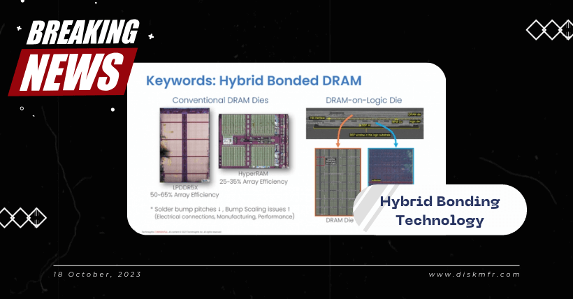
The most significant advantage of Hybrid Bonding is the ability to increase chip density. Currently, the latest memory chips, such as LPDDR5X, only achieve a 50% unit array efficiency. With the implementation of Hybrid Bonding, DRAM array chips and peripherals can be produced separately, similar to NAND, resulting in a substantial increase in chip density. This means more storage capacity without a significant increase in the physical size of the chip.
2. Improved Performance
With increased chip density, the overall performance of DRAM is expected to improve. This means faster data access, reduced latency, and a smoother user experience for a wide range of electronic devices, from smartphones to data centers.
3. Cost-Efficiency
As Hybrid Bonding technology enables more efficient use of materials and resources, it has the potential to reduce production costs. Lower costs can be passed on to consumers, making high-capacity DRAM more accessible and affordable.
4. Sustainability
Efficiency and resource optimization are not only cost-effective but also environmentally friendly. Reducing waste and improving the overall efficiency of semiconductor production can contribute to a more sustainable tech industry.
06
The Road Ahead
In conclusion, the introduction of Hybrid Bonding technology into the world of DRAM promises a brighter and more efficient future. This innovation addresses some of the key challenges currently faced by the DRAM industry, such as limited capacity and increased demand for higher performance.
As industry leaders like Samsung, SK Hynix, and Intel prepare to embrace this transformative technology, we can expect to see a new generation of DRAM products that not only meet but exceed our expectations. With enhanced density, improved performance, cost-efficiency, and sustainability, Hybrid Bonding is set to reshape the landscape of semiconductor technology.

Recommended Reading:


