Why is Japan in a hurry to revive the semiconductor industry? Chip manufacturing has jumped from 40nm directly to 2nm. What is Japan thinking? With Moore’s Law nearing its end, where will chip technology development go? Why is time cost becoming increasingly important? What role will AI play in semiconductor development? Why avoid a chip war?…
Mentioning Japan’s semiconductor industry often evokes key terms: “lost three decades,” Plaza Accord, dominance in upstream materials…
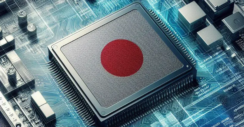
The Japanese semiconductor industry, which has been relatively dormant for almost 30 years, has been exceptionally active in the past two years. The most eye-catching development is Rapidus, a semiconductor manufacturer formed by a coalition of eight leading Japanese companies, aiming directly at 2nm, intending to challenge TSMC and Samsung.
Japan is placing all its bets on semiconductor revival.
This year, Chris Miller’s “Chip Wars” became a hot book in the semiconductor industry. Across the sea in Japan, another book shares the limelight with “Chip Wars” on the shelves, namely, Toshihiro Hikita’s “Semiconductor Super-Evolution Theory.”
Author Toshihiro Hikita is a professor in the Graduate School of Electrical Engineering and Systems Science at the University of Tokyo. He has worked at Toshiba, Keio University, and the University of California, Berkeley. Currently a professor at the University of Tokyo, he’s a key figure in Japan’s semiconductor revival plan and is regarded by some media as a pioneer in 3D stacking technology.
01
Japan’s semiconductor revival: Direct push towards 2nm
The Japanese semiconductor industry has been almost dormant for about 30 years, lagging approximately 10 years behind TSMC and Samsung in chip manufacturing technology, currently operating at the 40nm process node.
Driven by a sense of urgency due to the lag in advanced processes, Japan’s eight major conglomerates established Rapidus last August, collaborating with IBM to develop 2nm technology, aiming to construct one or multiple wafer fabrication plants in Japan for production.
Understanding Japan’s ambition to excel in advanced processes, but aiming for mass production of 2nm right away, what gives them the confidence?
Perhaps even Japan finds it hard to pinpoint the source of this confidence. More than confidence, it seems to be a pressing necessity—a “do-or-die” situation.
The global semiconductor market is anticipated to grow rapidly at a pace of 8% annually. By 2030, the market’s value could potentially double its current size, surpassing a value of over 100 trillion yen. Japan’s global market share in the semiconductor industry was as high as 50% in 1988, but it has now plummeted to just 10%. Remaining almost dormant for over 20 years, Japan has decided, at the risk of its national fate, to bet on the revival of its semiconductor industry.
02
What does Japan’s semiconductor revival require?
Merely relying on conventional strategies is challenging to recover from the lost 30 years. Anticipating the competitive stage and investing ahead of time has become crucial. To address this, the author presents three changes in the current industry in the second chapter titled “A Comeback.”
Firstly, a shift in the industry’s protagonist is evident. The battleground for logic chips is transitioning from general-purpose to specialized chips. Three reasons underlie this shift: the rapid surge in data and the complexity of AI processing are intensifying the energy crisis; the emergence of AI will amplify energy efficiency by over tenfold; semiconductor industry specialization allows companies to autonomously develop specialized chips based on their business models.
Secondly, market fluctuations. Every quarter-century, significant waves disrupt the semiconductor market, such as previous waves involving household appliances, PCs, and smartphones, with Japan seizing only the first wave. The impending fourth wave involves highly integrating cyberspace and physical space through the use of sensors, AI, and motors, creating a “digital twin” technology to construct a human-centric society, also known as “Society 5.0.”
Thirdly, a paradigm shift in technology. One shift is from von Neumann architecture to neural networks, and the other is from miniaturization to 3D integration. Chip miniaturization has almost reached its limit, while 3D integration can significantly reduce energy consumption in data transmission.
Moreover, these three changes fundamentally address energy issues. The sharp rise in energy consumption is attributed to semiconductors. Thus, the key to solving this problem lies in semiconductors—enhancing semiconductor energy efficiency.
To improve energy efficiency, the author proposes two key points: miniaturization technology and 3D integration.
The representative initiative in miniaturization is Rapidus. Unlike TSMC’s comprehensive production lines, Rapidus quickly produces the world’s most advanced products in small batches. It starts manufacturing at the 2nm process, using only the most cutting-edge 3rd generation technology.
Even within Japan’s industry, many question Rapidus’s strategy, considering it overly bold.
The author supports Rapidus’s strategy. Firstly, advanced technology is profitable; in fact, TSMC’s most lucrative aspect comes from its leading-edge technology.
Previously, even cutting-edge technology relied on low-cost competition for profitability. Now, as the number of early entrants into the market decreases annually, it becomes an oligopoly. However, demand for cutting-edge chips persists and expands, giving early entrants leverage in pricing.
Secondly, the 5nm market has been saturated by TSMC, Samsung, and Intel, making it difficult for new players to enter. The 2nm technology employs GAA rather than the FinFET technology used in 5nm and 3nm. Rather than expecting “old technology” to provide experience, starting afresh from the “new technology” seems more promising.
Moreover, instead of competing with major foundries, targeting small-batch orders they cannot cover allows coexistence and complementarity. Additionally, clients are expecting such services.
Besides miniaturization, 3D integration is another key aspect of enhancing efficiency.
As per Japan’s current situation, Japan lags far behind in miniaturization technology and needs to learn from overseas. However, in terms of materials and basic technology for manufacturing equipment used in 3D integration, Japan holds numerous advantages.
Specialized chip development entails long cycles and substantial funding. Creating a silicon compiler for programmable automated design chips might expedite hardware development. While the performance of automated design might score only 80, a fivefold increase in development efficiency is acceptable.
Between 2019 and 2020, the University of Tokyo established collaborative centers such as d.lab and the Research Organization for Advanced Systems (RaaS), aiming to complement Rapidus and collectively enhance energy and development efficiency tenfold.
Regarding energy efficiency, Rapidus pursues miniaturization, while the University of Tokyo focuses on 3D integration. Concerning development efficiency, Rapidus shortens production cycles, whereas the University of Tokyo studies methods to reduce design cycles.
03
How will chip technology evolve in the future?
“The Moore’s Law is dead.”
In recent years, countless individuals have raised doubts about this “golden rule” of chip development. Indeed, Moore’s Law has reached its limits. Some continue exploring miniaturization, referring to it as “deep Moore,” while others have started focusing on new values in other aspects, terming it “beyond Moore.”
The author’s choice aligns with the latter. With Moore’s Law nearing its end, the author believes that rather than extending the traditional technological path, embracing disruptive technology and researching its practical applications represents a significant upcoming opportunity.
The current challenge in chip development is the limitation faced in improving performance. As power, specifically heat, reaches its limit, no further enhancement in performance is achievable regardless of how much circuitry is integrated. The efficiency of power consumption per unit of processing, known as power efficiency, will determine the fate of Moore’s Law.
A side effect of miniaturization is an increase in power consumption by semiconductor components. Strategies to reduce power consumption involve three aspects: lowering voltage, reducing capacitance, and minimizing switching frequency. Reforms in materials, processes, and structures have been pursued to address these three aspects.
① From 2D to 3D
As data’s rapid growth encounters the Von Neumann bottleneck, communication between chips has become a crucial factor in reducing energy efficiency because data transmission consumes more energy than computation.
Chip computational performance increases by over 70% annually. To fully utilize the enhanced chip performance, chip-to-chip signal transmission speed should increase by 44% each year. However, in reality, chip-to-chip communication speed only increases by 28% per year.
How can this gap be bridged?
By reducing the distance between memory and processors while increasing the number of connections for reasonable-speed signal transmission. In other words, utilizing chip stacking for short-distance connections and communicating across the entire surface at an appropriate speed is why chips are evolving from 2D to 3D.
Silicon through-silicon vias (TSV) and magnetic coupling communication (TCI) technologies are new technologies born from this trend.
② From Horizontal to Vertical
3D integration started with memory, initially stacking two DRAMs in High Bandwidth Memory (HBM), then progressing to 4, 8, and 12 stacks. They were all horizontally stacked, referred to as “pancake” stacking.
However, theoretically, there’s another stacking possibility—vertical stacking, termed “sliced bread” stacking.
The sliced bread stacking is more advantageous than the pancake stacking. Firstly, it offers better heat dissipation; secondly, communication is more efficient.
③ Synchronous Design versus Asynchronous Design
Improving chip performance requires precise timing design. It involves calculating the impact of manufacturing component variances, power supply voltage, and temperature changes on signal propagation delay in logic circuits, as well as fluctuations during clock generation and timing disparities during distribution.
The cost and waste of current synchronous design practices are becoming prominent. Therefore, people are reconsidering the previously unfeasible asynchronous design.
While asynchronous design uses more transistors and wiring compared to synchronous design, it likely offers gains compared to the waste seen in synchronous design.
The author initially anticipated achieving asynchronous design at 7nm, but FinFET technology surpassed transistor performance expectations, leading to its non-implementation. As transistor structural reforms are ongoing, the application of asynchronous design might take some time.
In 1959, physicist Richard Feynman proposed that “there’s plenty of room at the bottom,” leading to the birth of microelectronics. Today, facing the imminent limit of Moore’s Law, the author says, “There’s plenty of room at the top,” implying that involving more people in chip development is crucial.
Currently, only large companies can develop specialized chips due to the industry’s emphasis on mass production cost-effectiveness. However, “time-effectiveness” is now also crucial.
Firstly, society is transitioning from capital-intensive to knowledge-intensive, where intelligence creates value, driving digital innovation. Semiconductors have transformed from low-cost components to essential tools in building society. Secondly, semiconductors have shifted from industrial infrastructure to societal infrastructure. This means semiconductors are more integrated into products like robots, and communication devices, which companies won’t easily replace.
Additionally, the author mentions several solutions such as agile development, silicon compilers, and chip automation design platforms, all of which offer new possibilities for chip development, especially for time-consuming and costly specialized chip development.
“Do Not Engage in Chip Wars”: A Voice from a Japanese Semiconductor Researcher
“Survival of the fittest.”
Darwin’s theory of evolution has been around for over 160 years, yet the forefront of science is unveiling more intricate mechanisms of evolution: support and cooperation.
The author once encountered the concept of “Super Evolution” on a television program.
About 5 billion years ago, Earth’s land was barren. Around 400 million years ago, plants covered the land. In the Cretaceous period, the appearance of something changed the diversity of terrestrial life significantly — flowers.
Flowers entice insects with pollen, and in return, the insects aid in pollination. They established a “symbiotic” relationship. Before this, plants were merely prey for insects.
Subsequently, flowers and insects began influencing each other, evolving due to each other’s presence, leading to a flourishing ecosystem.
This symbiosis, hidden beneath competition, better ensures the continuation of life, and this is the key to the development of the semiconductor industry.
A semiconductor giant is like a tree, but what’s more crucial is the soil nurturing life underneath, akin to a forest formed by numerous such trees.
A set of semiconductor manufacturing equipment consists of over 100,000 components, whereas a car has approximately 30,000 parts. Moreover, the inventory of over 100,000 parts in each equipment varies, with a diverse array of suppliers.
Therefore, a vast network encompassing multiple layers and spanning across industries has emerged around semiconductors. Furthermore, the intricate semiconductor manufacturing process requires constant collaboration, support, and adjustments among suppliers, manufacturers, and users, akin to an ecosystem within a forest.
The public often focuses solely on the towering trees, and media attention centers around the rise and fall of major companies. However, what truly sustains these large corporations is the rich soil, which represents the strength of an industrial ecosystem network. Japan’s strength in semiconductor manufacturing equipment and materials lies within this network.
This is also why TSMC chose Kumamoto, Japan, as the site for its new factory. Kumamoto’s history as an industrial land provides such fertile soil.
The Japanese semiconductor industry has long been committed to nurturing a “forest” that supports mutual aid, and interconnectedness, and now, these efforts are starting to attract global attention.
With the advent of TSMC’s new factory in Kumamoto, various associated investments and support from Japanese material and equipment suppliers have surfaced. The emergence of this colossal tree rejuvenates the underground network.
Hence, in Chapter Six, titled “Super Evolution,” the author posits that the key elements of the new era in semiconductors are international cooperation, international talent mobility, networks, symbiosis, and evolution.
As early as 20 years ago in 2003, the author, then a professor at Keio University in Japan, alongside Professor Hoi-Jun Yoo from KAIST in South Korea and Professor Zhihua Wang from Tsinghua University in China, reached a consensus. They believed that the future focus of the global integrated circuit industry would shift to Asia, where young Asians would play a significant role in the industry.
In pursuit of this vision, they established a small closed-door academic workshop called the KKT Workshop, involving graduate students from the three universities in Japan, South Korea, and China. This workshop, hosted annually by Keio University, KAIST, and Tsinghua University on a rotating basis, has persisted for over 20 years. As the author moved to the University of Tokyo, the students from Keio University transitioned to the University of Tokyo.
The author advocates against inciting chip wars and instead proposes building a chip network, outlining his vision for the future of the semiconductor industry.
Whether the Japanese semiconductor industry can experience a revival with Rapidus remains uncertain. But as the author asserts, “Everything is finally about to begin.


