Chips are hidden in electronic devices that can be found everywhere in the city, such as smartphones, computers, and home appliances, all of which rely on their control.
These tiny chips integrate circuits on a massive scale.
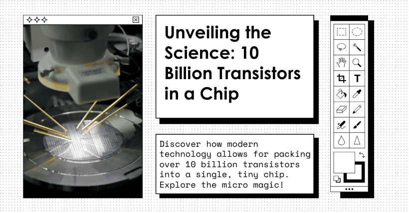
When magnified, the interior of the chip reveals a dense arrangement of circuits, similar to a tightly interwoven network of highways, as if a well-organized circuit city has been built on a very small scale.
How small is the inside of a chip? The smallest process size used in industry today, which is the smallest dimension we humans can create, has reached 3nm. The chip can integrate tens of billions of transistors.
01
The “multi-layer” approach to chip manufacturing
Are the countless nanoscale electronic components scattered across the chip made in advance and then placed one by one?
No! We can look at this issue from another angle. By observing vertically, it can be seen that the chip is made up of layers of sheet structures stacked vertically, each with different patterns. If each layer is made in advance and then stacked vertically, a two-dimensional structure can be assembled into a three-dimensional device, ultimately forming a chip with rich functionalities.
Now our goal has become how to create sheet structures with specific patterns. First, we need a sheet material that can be used to print circuit diagrams, commonly known as silicon wafers. This is a type of silicon with extremely high purity, which after processing, is cut into smooth, very thin discs.
Next, like carpenters, we need to find the right tools to carve the patterns. To create chips with complex internal structures and extremely small features, the size requirements for the processing tools are very high.
Cleverly, we have found light in this carving tool. Due to the rich wavelengths of light, we can use short-wavelength light to achieve extremely fine processing.
We aim to transfer the circuit patterns designed on blueprints onto silicon wafers through optical exposure, but since light does not affect silicon material, an intermediate material is needed. This material is a photoresist, which can interact directly with light.
To enable light to transfer the pattern information can be achieved by completely blocking or allowing light to pass through, creating patterns of light and dark. Light passes through a mask with circuit patterns, replicating the pattern information of the mask. After interacting with the evenly coated photoresist on the surface of the silicon wafer, the required pattern information appears on the silicon wafer.
The photoresist is the primary carrier medium for photolithography imaging and is divided into positive and negative types. Positive photoresist is easier to dissolve in the developer in the exposed areas, while negative photoresist is less soluble in the developer in the exposed areas.
Assuming a positive photoresist is used, once the exposure process is completed, the developer can dissolve the photoresist that has been exposed to light. Then, chemicals are used to dissolve the exposed silicon wafer, leaving the photoresist on the surface of the silicon wafer to protect it; this is known as the etching process.
We have now achieved our goal of obtaining a silicon wafer with specific circuit patterns. Throughout this entire process, the general idea is quite smooth, but chip manufacturing, a precision engineering feat representing the pinnacle of human intelligence, involves numerous stringent requirements.
02
What limits the internal dimensions of a chip?
The main components of a chip are transistors, and a large chip can have tens of billions of transistors. The smaller the transistors we can make, the more components a chip can accommodate, and the lower the power consumption of the transistors will be.
In chip manufacturing, we aim to use light to create circuit patterns on a small scale. So, why can light achieve this effect? And what is the limit to light’s engraving capabilities?
Diffraction
The primary factor affecting the engraving standard of light is the diffraction effect of light. Light is an electromagnetic wave, and diffraction is inevitable during the photolithography process, resulting in a minimum feature size for the exposure area. The resolution of light, which is the ability of the photoresist to reconstruct patterns based on light irradiation, is thus limited.
When a beam of parallel light passes through a slit, it interferes with countless sub-waves during transmission, creating a diffraction pattern of alternating light and dark.
This means that when considering the propagation of light on a microscopic scale, the lit areas are no longer distinctly separate from unlit areas; instead, there is a blurred zone. The light emitted from an ideal point object, after passing the edge of an obstacle, deviates from the characteristic straight-line propagation of geometric optics and no longer forms an ideal image point.
This is because when the slit width is comparable to the wavelength of light, the wave nature of light takes center stage. Light can utilize its wave properties to bend around obstacles and disperse in space, resulting in a diffraction effect that causes the light to spread. This leads to exposure areas that are no longer precise, and there is a limit to the resolution of light.
Resolution
In the field of optical imaging, resolution is the ability to distinguish between the images of two adjacent points. Ideally, each point would produce a sharp image point, but due to diffraction, the actual result is a light spot of a certain size. If two light spots (diffraction patterns) overlap too much, the image points become difficult to distinguish.
Rayleigh proposed an effective criterion, and the resolution formula is:
This resolution expression describes the limit at which two light spots can just be resolved—when the maximum of one light spot coincides with the first zero of the other light spot. Here, λ is the wavelength of the illumination light.
NA stands for Numerical Aperture, which describes the lens’s ability to converge light, specifically the degree of deviation (convergence to a focus) after parallel light incidence, calculated as:
The Rayleigh criterion is commonly used to evaluate image quality, while the photolithography system images within the photoresist. The photoresist is a high-contrast imaging medium, and under certain exposure conditions, although the optical resolution has reached below the Rayleigh criterion limit, the photoresist can still produce good imaging results and achieve the processing goals.
The resolution of photolithographic imaging is defined as:
Rlitho is the pattern period resolvable by the photolithography system; k1 is the process factor.
Photolithography
In chip manufacturing, photolithography is the most complex, expensive, and critical process. It typically uses a projection photolithography system to project the circuit structure from a mask onto the surface of a silicon wafer.
Optical lenses can gather diffracted light to enhance image quality. In photolithography, to achieve as small a pattern as possible, a projection imaging objective with a reducing magnification ratio is used between the mask and the photoresist.
03
How to Sharpen Light as an Engraving Tool?
We now know that the minimum processing scale (resolution) of light determines how small a chip can be. How can we make the chip even smaller? We need to enhance the resolution to make the circuit city on the chip more sophisticated.
Based on the three terms in the photolithography resolution formula, we have three strategies to sharpen light as an engraving tool.
- Increase the Numerical Aperture of the Photolithography System: The greater the numerical aperture of the projection lens in a photolithography imaging system, the better the resolution. A specific implementation is to design an immersion lithography machine, which involves filling a high refractive index medium between the wafer and the final lens of the projection objective.
- Shorten the Wavelength: The wavelength used in the photolithography process has evolved through the G line (432nm), I line (365nm), KrF (248nm), and ArF (193nm) deep ultraviolet bands, and currently, extreme ultraviolet (EUV) lithography machines with a 13.5nm wavelength are in use.
- Reduce the Process Factor: By optimizing photolithography process parameters, such as improving lighting conditions, photoresist processes, and mask design, the process factor k1 can be reduced. These methods are known as Resolution Enhancement Techniques (RET).
Light is an electromagnetic wave, thus it carries information such as amplitude, phase, polarization state, and propagation direction. Resolution enhancement techniques in photolithography involve manipulating these four types of information to achieve finer structural patterns on the photoresist. For instance, off-axis illumination techniques can change amplitude and phase, optical proximity correction techniques can alter the amplitude of light waves, and source-mask optimization can adjust the propagation direction, amplitude, and phase of light waves.
Reviewing the development of lithography machines, we are indeed progressing along the path of continually reducing wavelengths. Observing the data in the table, even when the wavelength of the light source remains the same, we continue to decrease the process nodes, thanks to the numerical aperture, process factor, and other complex technologies.
Related:
- G-line, I-line, DUV, EUV: Key Lithography Terms Explained
- Understanding Optical Clarity in Semiconductor Films

Disclaimer: This article is created by the original author. The content of the article represents their personal opinions. Our reposting is for sharing and discussion purposes only and does not imply our endorsement or agreement. If you have any objections, please contact us through the provided channels.


