Today, the parameter count of large models has been skyrocketing into the billions.
In just two years, the computational power required for large models has increased by 1,000 times—far outpacing the speed of hardware iteration. Currently, mainstream AI large model solutions rely on GPU clusters.
However, single-chip GPUs face obvious bottlenecks: First, the physical size of a single chip limits the number of transistors; even with advanced process technologies, performance gains are approaching the limits of Moore’s Law. Second, in multi-chip interconnects, the latency and bandwidth loss from data transfers between chips prevent linear scaling of overall performance.
This is why, when dealing with trillion-parameter models like GPT-4 and Ernie Bot, even stacking thousands of NVIDIA H100s cannot escape the dilemma of “insufficient computing power and skyrocketing electricity costs.”
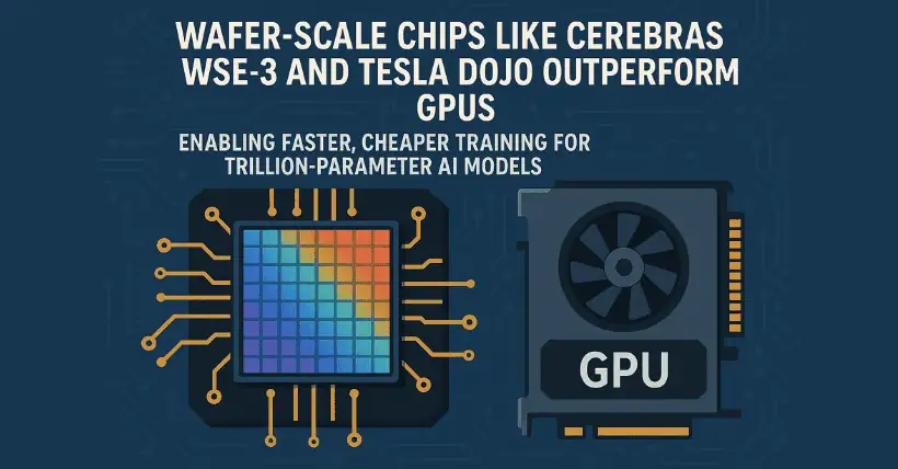
At present, the AI training hardware industry is split into two camps: dedicated accelerators using wafer scale integration (e.g., Cerebras WSE-3 and Tesla Dojo), and GPU clusters based on traditional architectures (e.g., NVIDIA H100).
Wafer scale chips are considered the breakthrough path of the future.
01
Wafer Scale Chips: Two Major Players
In traditional chip manufacturing, a wafer is cut into many small dies after photolithography, and each die is individually packaged into a complete chip.
To enhance chip performance, manufacturers aim to increase chip area. Currently, single-die compute chips have an area of approximately 26×33 = 858 mm², nearly the size of an exposure window. However, the maximum chip size cannot exceed the exposure window, which has remained unchanged for years, becoming a key constraint on chip performance growth.
Wafer scale chips offer a new approach. Instead of cutting the wafer, they use it as an interconnected substrate, integrating and packaging multiple designed dies directly on it to create one massive chip.
The circuit units and metal interconnects on an uncut wafer are more densely packed, resulting in higher bandwidth and lower latency interconnects—creating a more powerful compute node via high-performance interconnects and dense integration. At the same compute power, clusters based on wafer scale chips occupy 10–20 times less space and consume over 30% less power than GPU clusters.
Two companies have already developed wafer scale chip products.
One is Cerebras. Founded in 2015, the company launched WSE-1 in 2019 and has now released its third-generation wafer scale chip—WSE-3.
WSE-3 uses TSMC’s 5nm process, contains a staggering 4 trillion transistors, has 900,000 AI cores, 44GB of on-chip cache, and supports up to 1.2PB of off-chip memory.
WSE-3 can train next-generation frontier models 10 times larger than GPT-4 or Gemini. With four units in parallel, it can complete training for a 70-billion-parameter model in one day, supporting up to 2,048-way interconnects.
All of this is integrated on a single 215mm × 215mm = 46,225 mm² wafer.
To highlight the contrast: compared to NVIDIA H100, WSE-3 has 880 times the on-chip memory, 7,000 times the single-chip memory bandwidth, 52 times the core count, and 3,715 times the on-chip interconnect bandwidth.
The other player is Tesla. Tesla’s wafer scale chip is named Dojo, an initiative started by Elon Musk in 2021.
Tesla’s Dojo follows a different path from Cerebras, using a chiplet architecture where 25 proprietary D1 dies are integrated onto a wafer-sized substrate.
Each D1 die, at 645 mm², houses 50 billion transistors and provides 362 TFlops BF16/CFP8 compute power. Together, a single Dojo unit delivers 9 petaflops of performance and 36TB/s bandwidth.
Dojo is custom-built for training Tesla’s Full Self-Driving (FSD) models. The system architecture scales from 25 D1 dies → 1 training tile → 6 tiles per tray → 2 trays per cabinet → 10 cabinets form one ExaPOD supercomputer, capable of 1.1 exaflops of compute power.
02
Wafer Scale vs. GPU: A Comparison
Since single-chip GPUs and wafer scale chips have diverged, let’s compare Cerebras WSE-3, Tesla Dojo, and NVIDIA H100 as representatives of their respective architectures.
Key metrics for evaluating AI training chips include:
- FLOPS (Floating Point Operations Per Second) – the raw compute capability, crucial for matrix-heavy deep learning tasks.
- Memory Bandwidth – determines data access and processing speed.
- Latency and Throughput – affect efficiency in handling large data loads and parallel models, impacting real-time performance.
✅ Compute Performance
WSE-3 showcases unique potential with its monolithic architecture.
Its peak FP16 training performance is 125 PFLOPS, supporting models with up to 240 trillion parameters—without requiring model partitioning. This makes it ideal for streamlined processing of ultra-large models.
Unlike traditional GPUs that rely on hierarchical memory (which may cause bottlenecks), WSE cores run independently and access local memory directly, improving throughput.
NVIDIA H100, using a modular distributed approach, delivers 60 TFLOPS FP64 compute per chip. A system of eight interconnected H100s offers over 1 exaflop of FP8 AI performance.
However, distributed setups introduce communication overhead. While NVLink and HBM3 memory help reduce latency, inter-GPU communication still affects training speed for massive models.
WSE-3 excels in large-model training. A 2048-unit WSE-3 cluster can train Meta’s 70B-parameter LLaMA 2 LLM in just one day—30 times faster than Meta’s original cluster.
✅ Latency and Throughput
WSE-3’s monolithic structure avoids multi-chip data transfers, significantly reducing latency and enabling massive parallelism and low-latency core-to-core communication. Compared to traditional GPU clusters, WSE-3 reduces software complexity by up to 90% and GenAI inference latency by over 10x.
Dojo’s Training Tile also cuts communication costs thanks to wafer scale integration. Though die-to-die interconnects still create some latency, Dojo achieves 100ns inter-chip latency and can process 1 million 36-fps video streams simultaneously, optimized for autonomous driving training.
H100, built on the Hopper architecture, is currently the most powerful AI training GPU with 18,432 CUDA cores and 640 tensor cores. NVLink and NVSwitch enable fast GPU communication. Despite the scalability of multi-GPU systems, data transmission still causes latency—even with NVLink 4.0’s 900GB/s per GPU bandwidth, latency is higher than in wafer scale systems.
While wafer scale systems offer low-latency, high-throughput workloads, they face limitations in scalability, high manufacturing costs, and limited flexibility for general workloads.
✅ Cost-Effectiveness
Hardware costs vary by architecture and use case.
Tesla’s Dojo supercomputer reportedly costs $300M–$500M. Its approach combines mature wafer processing with advanced packaging (using TSMC’s Info_SoW), enabling wafer scale compute without pushing process limits—ensuring good yields and easier chiplet upgrades.
Cerebras WSE systems have higher R&D and manufacturing costs due to complex design and advanced processes. Reports estimate the cost of one WSE-2 system at $2M–$3M.
In contrast, NVIDIA GPUs have lower individual costs. The A100 (40GB PCIe) is priced around $8,000–$10,000, while the 80GB SXM model costs $18,000–$20,000. This makes NVIDIA a more attractive choice for companies building AI infrastructure in early stages. However, long-term issues like high power consumption and multi-chip performance bottlenecks can drive up operating costs.
Overall, while WSE-2 offers ultra-high compute density for massive AI models, A100 has clear cost advantages for institutions needing scalable GPU solutions in large data centers and cloud deployments.
03
Conclusion
In conventional setups, more cluster nodes mean larger clusters, which increases communication overhead and reduces efficiency.
That’s why NVIDIA’s NVL72 enhances node integration density (compute density) within a rack—packing more GPUs into one rack to control cluster size and improve efficiency.
This is NVIDIA’s balanced solution between yield and cost. But if NVIDIA continues down this path, further compute density improvements will inevitably lead toward wafer scale designs, since wafer scale chips currently offer the highest integration density for compute nodes.
Wafer scale chips hold immense potential.
Source: Internet

Disclaimer: This article is created by the original author. The content of the article represents their personal opinions. Our reposting is only for sharing and discussion purposes and does not imply our endorsement or agreement. If you have any objections, please get in touch with us through the provided channels.


