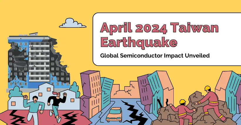
According to the meteorological department in Taiwan, as of 10:37 p.m. on April 3, there have been 216 earthquakes centered in Hualien County, Taiwan, and the nearby sea area since the main quake. Regarding the impact of this earthquake on the semiconductor industry chain, global market research firm TrendForce has surveyed the damage and operational status of various factories. It points out that the DRAM (Dynamic Random Access Memory) industry is mostly concentrated in the northern and central parts of Taiwan, while the foundry industry is spread across the north, central, and southern regions. The earthquake on the morning of the 3rd was between 4 to 5 on the Richter scale in the northern Linkou area, with other areas experiencing around magnitude 4. Factories are progressively conducting shutdown inspections. Although the inspections are not yet complete, so far, no significant damages to the equipment have been found.
Taiwan is the world’s largest base for wafer production. In 2023, Taiwan accounted for about 46% of the global wafer foundry capacity. The industry is currently most concerned about whether the global chip supply will be disrupted and whether the chip shortage situation of 2021 will reoccur.
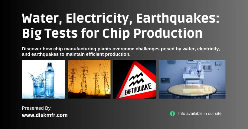
The chip industry’s challenges this year extend beyond earthquakes, including shortages of electricity and water…
01
Chip Manufacturing is Unsustainable Without Water.

The production facilities that the United States and Europe are announcing or building are located in regions already facing severe water stress. Intel, TSMC, and Samsung are all constructing new factories in the southwestern United States, an area that has been in a state of drought since 1994. In 2021, the U.S. Bureau of Reclamation announced a water shortage in the Colorado River basin for the first time. Future climate change scenarios suggest that over 40% of all new semiconductor manufacturing facilities announced since 2021 will be in watersheds that may experience high or extremely high water stress.
Amid efforts to reduce greenhouse gas emissions causing global warming, the energy-intensive nature of semiconductor manufacturing and its significant carbon footprint have garnered considerable attention. It turns out that we are both thirsty and hungry. Our industries consume a vast amount of water, up to 264 billion gallons annually, and this resource may become scarcer with climate change. A single wafer fab can use tens of millions of gallons of water daily. To put this in perspective, the average water use in the U.S. is about 310 liters per person per day, and 10 million gallons is equivalent to the daily domestic water use of a small city with a population of 122,000.
In short, climate change and water scarcity are posing short-term and long-term risks to semiconductor manufacturing.
Water security is becoming an increasingly important factor affecting the credit status of semiconductor companies. Improper management of water resources can disrupt operations, harm financial performance, and potentially affect customer relationships. Broadly speaking, given the integrated nature of the semiconductor supply chain, any potential production disruption could impact its end markets.
Climate change is testing chip manufacturers. As processing technology advances, the absolute and per-unit water usage of semiconductor companies is increasing. At the same time, climate change is increasing the frequency of extreme weather, droughts, and variability in precipitation, limiting chip manufacturers’ ability to manage production stability.
S&P Global Ratings believes that water security will become an increasingly important factor affecting the credit status of semiconductor companies. While most companies have been adept at managing this issue so far, increasing and frequent water shortages could overwhelm entities’ contingency plans.
Driven by capacity expansion and demand for advanced process technologies, the semiconductor industry’s water usage is expected to grow annually by a mid-to-high single-digit percentage.
For instance, after TSMC upgraded to the 16 nm process node in 2015, its unit power consumption increased by more than 35%, mainly due to the transition to advanced nodes requiring more manufacturing processes. There is a direct correlation between water usage and chip complexity because wafer fabs use ultra-pure water (freshwater treated to a very high purity) to rinse the wafers between each process step. The more advanced the semiconductor, the more process steps, and the more water consumed.
TSMC’s water security issues are significant but moderate compared to its peers. Water scarcity will not affect the foundry’s operations within the next three years, but beyond that, it is uncertain. Capacity expansion and technological development could leave TSMC with less leeway to withstand severe drought. Predictions indicate that by 2030, TSMC’s demand for water could double from its 2022 levels.
Taking Taiwan as an example, from October 2020 to June 2021, Taiwan experienced its most severe drought in 56 years. This was due to the absence of typhoons in 2020 and limited rainfall in the spring of 2021, causing reservoir levels to drop below 5% of their capacity. Authorities imposed water restrictions for about two months, affecting over one million households and businesses. The government shut off water supplies for two days a week in the hardest-hit areas, including Taichung, Taiwan’s second-largest city. A quarter of the island’s rice planting areas lacked irrigation. Local reports indicate that officials asked the tech industry, especially the semiconductor sector, to reduce water usage by 20%. Hydropower stations were also disrupted, leading to two major power outages in May 2021.
With the inevitable shift towards more advanced semiconductor process technologies, the requirements for water purity are also expected to increase. This means that TSMC might need to filter out more water that does not meet its increasingly stringent purity standards. This could limit TSMC’s ability to further improve its water recycling rate. The global tech hardware supply chain relies on a few major chip manufacturers. A reduction in operations at one of these companies could affect the production of many downstream businesses. The global chip shortage during the pandemic highlights the complexity and vulnerability of the tech supply chain to event risks.
02
Addressing Risks, Recognizing the Necessity for Sustainable Development
Semiconductor production requires large amounts of water and energy, most of which are treated and discharged as wastewater. As manufacturers seek to expand production scales and build new facilities to meet unprecedented demand levels, it is vital to remind the industry of the importance of efficient wastewater treatment.
Semiconductor manufacturing involves a wide and complex array of slurries and chemicals, necessitating strict wastewater separation, treatment, and recycling systems. Dealing with sludge containing metals and other hazardous wastes presents a challenge, and adhering to environmental regulations such as wastewater discharge standards can incur substantial costs.

The compounds involved in semiconductor production include hydrofluoric acid used for cleaning and etching photocomponents, as well as ammonia, ammonium fluoride, hydrogen peroxide, hydrochloric acid, sulfuric acid, and phosphoric acid used for rinsing. Cleaning semiconductor wafers, the most water-intensive part of the process, produces fluoride-rich wastewater, which requires neutralization with lime.
If an earthquake above magnitude 4 occurs in a region of Taiwan, the first action for chip manufacturers is to evacuate all employees from clean rooms and factories, waiting for the main quake to cease. The next steps include remotely monitoring the factory through a central control system to detect fires, toxic gas, or any chemical leaks that could lead to serious accidents. If the situation is safe, equipment, facilities, and materials teams can return to designated sites and begin physical inspections of the equipment.
The first task is to determine if the wafers being processed in the equipment are intact. If so, they can be reworked later. However, if the wafers are broken, engineers need to carefully clean the equipment room before restarting the machines. Next, they run a batch of control wafers to ensure the machines are functioning correctly before bringing them back online. These procedures must be meticulously carried out, and full production recovery takes time.
An equipment supplier manager stated, “It might take several hours to days or even weeks for all processes to return to normal, depending on the severity of the situation.” Industry insiders mention that all types of lithography machines typically take longer to restart than other chip manufacturing equipment. “Re-calibrating the lithography machine’s deviations after an earthquake is always a challenge. You need substantial support from equipment suppliers and specific tools. It requires high precision, and you can’t rush to resume the lithography machine.” This is where the professional ethics that Taiwanese engineers take pride in come into play.
An equipment engineer said, “If it happens on a holiday or outside normal working hours, all employees will return to the factory in less than an hour.” He also recalled working continuously for 48 hours to ensure production efficiency, ensuring his station was back to normal operation after another incident. “The rapid recovery is also closely related to the work culture in Taiwan’s chip industry…”
After an earthquake, factory, equipment, and materials engineers, as well as suppliers, work overtime during national holidays to restore production as quickly as possible. “We have to do a lot of inspections and recalibrations. I can assure you that all engineers in Taiwan are on duty, rushing out like wasps from a nest to help get the production tools back online,” said a manager.
03
Summary of Experience
Water is becoming increasingly valuable and scarce. Semiconductor manufacturing requires a large amount of water, primarily for the ultra-pure water needed for the production process itself. Water in factories has many other uses as well: cooling, washing, point-of-use emission reduction, and fire suppression. The amount of water drawn by a factory is equivalent to the water usage of tens of thousands of households, and now many wafer fabs are located in regions with strained water resources.
What can we do? Universal standards for water use, reuse, treatment, and recycling are necessary. Climate change will have negative impacts on water supply in many regions where semiconductor facilities are produced. Understanding the balance between recycling efficiency, energy use, and carbon footprint is also crucial. As production increases, innovative approaches involving wafer fabs, and local, and national governments are needed to manage this water risk.
Related:
- Waterproof USB Tech Explained: Uses and Key Insights
- Why NVIDIA Chips Rely on Microchannel Cooling Tech

Disclaimer: This article is created by the original author. The content of the article represents their personal opinions. Our reposting is for sharing and discussion purposes only and does not imply our endorsement or agreement. If you have any objections, please contact us through the provided channels.


