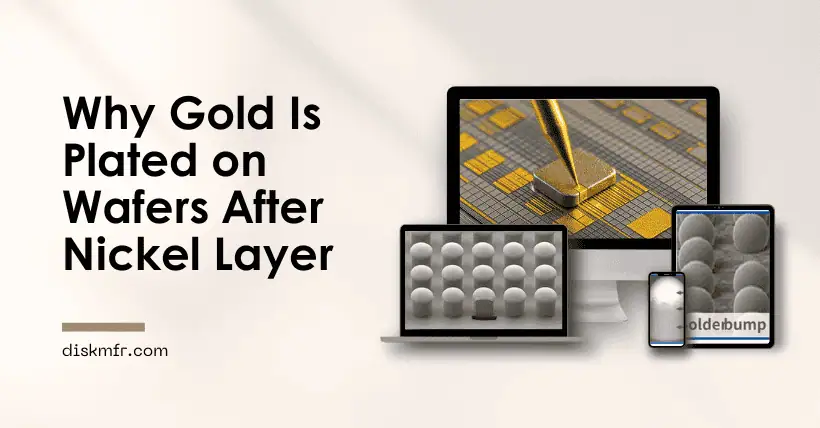
Why is nickel plated on top of copper after copper plating, and then gold plated on top of nickel? What is the general electroplating sequence?
Electroplating copper → Electroplating nickel → Electroplating gold → Electroplating solder balls — the functional roles of this four-layer metal structure:
Copper (Cu): Conductive layer, low resistance, easy to electroplate, inexpensive.
Nickel (Ni): Diffusion barrier layer, prevents Cu from diffusing into the gold layer, improves mechanical hardness.
Gold (Au): Anti-oxidation and enhances solderability, ensures reliable bonding afterward.
Solder ball: Soldered onto the package substrate.
Why is gold plated on top of nickel?
Nickel easily forms an oxide layer in air, and this oxide layer is an insulator, which affects the stability of the solder joint between nickel and the solder ball. Plating a layer of gold acts like putting anti-oxidation armor on the nickel surface. When the solder ball is finally plated, the gold is absorbed by the solder, allowing the solder ball to form a stable weld with the nickel.
Why do some use nickel-palladium-gold?
Palladium has a similar effect as gold. Previously, palladium was cheaper than gold, so it was used to replace some of the gold. In this case, only a very thin layer of gold is needed.
Related:

Disclaimer:
- This channel does not make any representations or warranties regarding the availability, accuracy, timeliness, effectiveness, or completeness of any information posted. It hereby disclaims any liability or consequences arising from the use of the information.
- This channel is non-commercial and non-profit. The re-posted content does not signify endorsement of its views or responsibility for its authenticity. It does not intend to constitute any other guidance. This channel is not liable for any inaccuracies or errors in the re-posted or published information, directly or indirectly.
- Some data, materials, text, images, etc., used in this channel are sourced from the internet, and all reposts are duly credited to their sources. If you discover any work that infringes on your intellectual property rights or personal legal interests, please contact us, and we will promptly modify or remove it.


