
Common PCB Rules. In PCB design, it is necessary to follow many rules to ensure the quality of the PCB. Here are a few common design rules that should be kept in mind. #Engineer #Chip #PCB.
01. Ground circuit rule
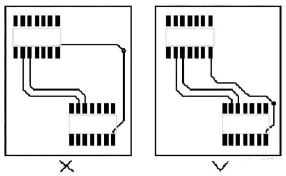
The minimum loop rule requires that the area enclosed by the signal line and its return path should be as small as possible. The smaller the area, the less radiation to the outside and the less susceptibility to external interference. When dividing the ground plane, it is necessary to consider the distribution of the ground plane and important signal traces, to prevent issues arising from slots in the ground plane, and so on.
02. Impedance matching check rule
The wiring width of the same network should be consistent. Changes in line width can cause uneven impedance in the circuit. This can cause reflections at high transmission speeds, which should be avoided as much as possible during design. In some cases, such as with connector leads or BGA package leads, it may be impossible to avoid changes in line width. In such cases, the effective length of the inconsistent portion should be minimized as much as possible.
03. Shielding protection
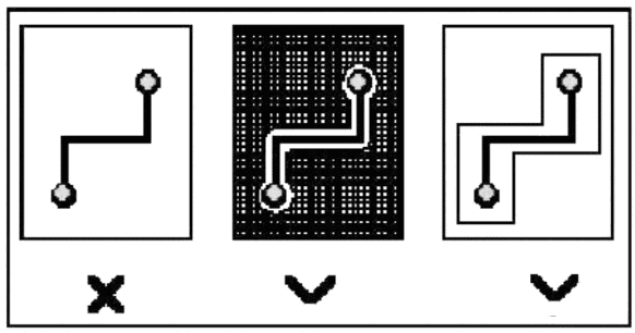
The corresponding ground loop rule is also aimed at minimizing the area of the signal loop. This is more common for important signals such as clock and synchronization signals. For particularly important and high-frequency signals, a shielded design with coaxial copper cable should be considered. This involves isolating the line above, below, left, and right with ground lines, and ensuring effective integration of the shielded ground with the actual ground plane.
04. 3W Rule
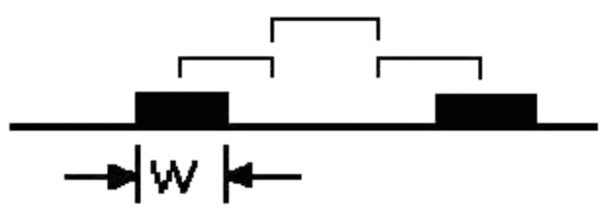
To reduce crosstalk between lines, it is important to ensure sufficient spacing between them. When the center-to-center distance between lines is not less than 3 times the line width, 70% of the electric field can be kept from interfering with each other, which is referred to as the ‘3W rule’. Using the spacing of IOW, 98% of the electric field can be kept from interfering with each other.
05. 20H Rule
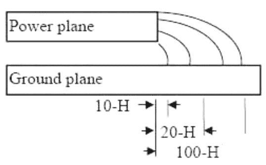
Due to the varying electric field between the power plane and the ground plane, electromagnetic interference is radiated outward at the edge of the board, which is called the edge effect. The solution is to shrink the power plane so that the electric field only conducts within the range of the ground plane. By a unit of H, if the power plane is shrunk by 20H, 70% of the electric field can be confined within the edge of the ground plane; if it is shrunk by 100H, 98% of the electric field can be confined within it.
06. Cable direction control
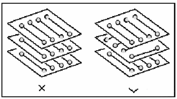
That is, the wiring direction of adjacent layers should form an orthogonal structure, avoiding the same direction of different signal lines in adjacent layers to reduce unnecessary interlayer crosstalk. (Signals in adjacent layers only need to be non-parallel, not necessarily orthogonal, depending on the wiring space.) When space is limited, especially for high-speed signals, inserting ground planes to isolate each wiring layer and using ground lines to isolate each signal line is recommended.


