
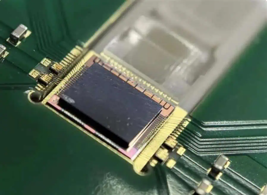
Yesterday, the China National Information Optoelectronics Innovation Center announced that a collaborative team with Pengcheng Laboratory has developed and verified a 2Tb/s silicon photonics interconnect chiplet.
This is also the first time in China that the 3D silicon-based optoelectronic chiplet architecture has been verified, achieving a unidirectional interconnect bandwidth of up to 8×256Gb/s per chip.
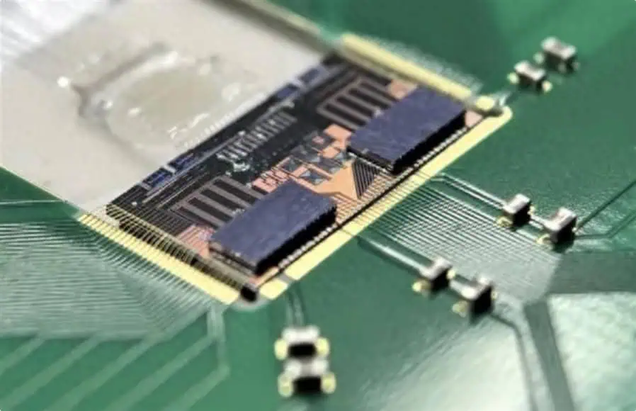
According to reports, the team advanced their 2021 1.6T silicon photonics interconnect chip, developing over 200G single-channel driver and TIA chips compatible with silicon photonics by breaking through optoelectronic collaborative design and simulation methods.
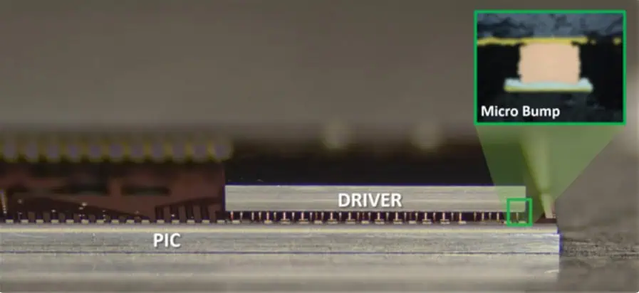
They also overcame technical challenges with silicon-based optoelectronic 3D stacking packaging and formed a comprehensive 3D chiplet integration solution based on silicon photonics.
In system transmission tests, the 8 channels maintained a TDECQ within 2dB at the next-generation optical module standard 224Gb/s PAM4 optical signal rate.
With further link balancing, the system can support rates up to 8×256Gb/s, achieving a unidirectional interconnect bandwidth of up to 2Tb/s per chip.
Currently, as chip technology advances and processes shrink, various effects due to interconnect lines significantly impact chip performance.
Silicon photonics technology can convert electrical signals into faster optical transmissions, providing faster speeds, longer distances, and reduced power consumption and latency.
Industry giants like Huawei, TSMC, Intel, IBM, and Oracle are all promoting silicon photonics industrialization, which may become a large-scale industry similar to integrated circuits in the future.
Related:

Disclaimer: This article is created by the original author. The content of the article represents their personal opinions. Our reposting is for sharing and discussion purposes only and does not imply our endorsement or agreement. If you have any objections, please contact us through the provided channels.


