
How will the future of semiconductors evolve?
With the new crown epidemic hitting the global supply chain, semiconductors have taught practitioners a real lesson. A segment of the population, after being the first to understand the causes of the chip shortage, discovered that it is possible to install more than 2 trillion transistors on a chip after constant attempts, and will also find that the future of Moore’s Law depends largely on where to put the wires, how small to make the transistors, etc.
Therefore, revisiting the content related to semiconductors in the past year, IEEE made the following points to summarize.
When and in what way will the chip shortage end?

It often happens to some automakers that even though they have hedged their risk by adding multiple suppliers, those suppliers or companies upstream of those suppliers may all be using products from the same small group of semiconductor fabs.
In retrospect, automakers panicked when the outbreak hit and canceled orders. Then, when people seemed to want to buy cars, they found that all the display drivers, power management chips, and other low-margin stuff they needed had been swept up in the “work-at-home learning and living” consumer boom. When automakers plan to re-purchase chips, the long line is almost a year away, which in turn has caused panic.
Chipmakers do their best to meet demand and quickly launched a wave of expansion, but the expansion of the main capacity in the more profitable advanced process chips, rather than those required by the automotive industry mature process chips. The latest data from SEMI, the chip manufacturing equipment industry association, shows that sales of semiconductor equipment in 2021 will exceed $100 billion, which is unprecedented.
And automakers have learned their lesson. 2021 summer, in Malta, N.Y., the GeChip eight factory (GlobalFoundries Fab 8) and the automotive electronics industry-linked, and finally, GeneChip signed a deal with Ford, BMW.
The next generation of chips will be powered by the following transistors
Transistors can be made as small as you want, but if you can’t connect them to each other, it doesn’t make sense. So Arm and the Belgian research institute Imec spent several years looking for this connection. The best solution they found was to bury the interconnects that deliver power to logic circuits (not data) on the surface of the silicon wafer and have them connect to a power distribution network on the back of the chip. This research trend is suddenly in the news because Intel seems to have expressed similar words, “Oh yeah, we’ll definitely be doing that in 2025.”
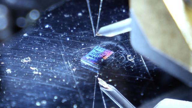
Cerebras’ new AI chip adds 1.4 trillion transistors

What has 2.6 trillion transistors, consumes 20 kilowatts of power, and has enough internal bandwidth to play a billion movies on Netflix? This is, of course, the second generation of the largest chip ever made. Last April, Cerebras Systems unveiled a version that used more advanced chip manufacturing technology to surpass the previously introduced AI processor. The result was a chip that more than doubled its memory to 40GB, increased the number of processor cores to 850,000 from the previous 400,000, and had 1.4 trillion more transistors.
While all of this is incredible, figuring out what it can be used for is what’s important. Cerebras showed a way that computers can use it to house a second-generation wafer-scale engine, Wafer ScaleEngine, to train neural networks with up to 120 trillion parameters. For reference, the massive GPT-3 natural language processor has 175 billion parameters of neural networks. In addition, today one can connect to 192 such computers simultaneously.
Of course, Cerebras’ computers are not the only ones used to handle huge AI training efforts. sambaNova is also pursuing this, and apparently, Google is also looking at some very large neural networks.
IBM launches the world’s first 2nm node chip

IBM claims to have developed a 2nm node chip and expects to enter production in 2024. With that in mind, leading chipmakers TSMC (TSMC) and Samsung (Samsung) are fully engaged in developing a 5nm node chip, possibly testing the waters for a 3nm node chip development in 2022. As mentioned last year, what most people call the technology process node has nothing to do with the size of any part of the transistor it is constructed from. Therefore, whether IBM’s development process is superior to that of its competitors will depend on the combined aspects of density, power consumption, and performance.
What really matters is that IBM’s process is yet another endorsement of the nanosheet transistor as the future of silicon materials. The major chip makers are moving at their own pace from today’s FinFET designs to nanosheets, so it is clear that the coming of the nanosheet era is inevitable.
RISC-V star rises among global chip developers

The news isn’t all about transistors; processor architecture is also becoming more and more important. The brain of a smartphone may be based on the Arm architecture, and a laptop and the server it’s connected to may be based on the x86 architecture. But a group of fast-growing companies, especially those based in Asia, are looking to an open-source chip architecture called RISC-V. Its uniqueness is that it allows startups to design custom chips without paying expensive licensing fees for proprietary architectures.
Even big companies like Nvidia are laying out RISC-V, and Intel predicts RISC-V will boost its foundry business. Chinese companies are particularly bullish on RISC-V as a possible path to independence in an increasingly polarized technology environment. Alibaba has also said it will provide source code for its RISC-V core.
New silicon optical chip 1,000 times faster than transistor

While certain types of optical computing are gradually being realized, such computer switching, described by Russian and IBM researchers last October, is likely to occur only in the distant future. Relying on substances such as exciton-exciton polaritons and Bose-Einstein condensates, the device switches at a rate of about 1 trillion times per second. The switching speed is so fast that light can only travel about a third of a millimeter before the device switches again.
New DRAM can accelerate the development of artificial intelligence

One of the big problems with artificial intelligence is that its data travels too far down the path. Of course, this distance is measured in millimeters, but now it’s a long distance. Now, engineers have come up with a number of ways to shorten that distance.
Instead of using a silicon transistor and a metal capacitor on top to make DRAM, a second transistor could be used as a capacitor while built on top of a silicon wafer of an oxide semiconductor. Two research groups have shown that these transistors can hold data storage longer than ordinary DRAM and can be stacked in layers on top of silicon, making the path between the processor and important data much shorter.
Intel announces big processor architecture changes

Last August, Intel announced the company’s biggest processor architecture advancements in 10 years, including two new x86 CPU core architectures — directly named Performance Core (P-core) and Efficiency Core (E-core). These cores are integrated into Alder Lake, a “performance hybrid” processor family that includes new technologies that will enable the upcoming Windows 11 operating system to run the CPU more efficiently.
Raja Koduri, Intel’s senior vice president and general manager, said at the time, “This is a great time to be a computer architect.” Intel’s new architecture and SoCs “demonstrate how the architecture will meet the demand for higher computing performance as workloads from the desktop to the data center become larger, more complex and more diverse than ever before.”
The U.S. takes strategic steps toward land-based electronics manufacturing

U.S. lawmakers are worried about China, Taiwan, and South Korea, the only two places that can make the most advanced logic chips, and they have begun efforts to promote cutting-edge chip manufacturing in the United States. TSMC, Samsung, and Intel have already begun making significant investments in chip plants. China and South Korea, of course, are also making major domestic investments, as are Europe and Japan.
Abishur Prakash, a geopolitical futurist at the Centre for the Future of Innovation in Toronto, notes that this is all part of a broader economic and technological nationalism on a global scale. Some believe these “geopolitical shifts are short-term, like a byproduct of a new epidemic that will calm down at some point,” he said in May in IEEE Spectrum, “and that view is wrong. The direction countries are going now is hardly going to succeed.”
How will the camera chip develop next?

A camera chip from French startup Prophesee and major imager manufacturer Sony, unlike conventional imagers, does not capture frame after frame with each tick of the clock. Instead, it records only the changes in the scene. This means that there will be lower power consumption and faster response time.
From IEEE


