NAND flash has been the dominant technology for low-cost and high-density data storage applications for decades. This non-volatile memory is found in all major electronic end markets, including smartphones, servers, PCS, tablets ,and USB drives.
From EDN
In the traditional computer memory hierarchy, NAND flash is located farthest from the CPU and is relatively cheap and slow compared to SRAM and DRAM.
The importance of flash memory is reflected in its substantial share of global semiconductor CAPEX, about one-third. Its success is tied to its ability to expand storage density and cost, which is a major driver of NAND flash technology. About every two years, the NAND flash industry is able to dramatically increase bit storage density.
Along the way, the industry has introduced a number of technological innovations to keep the trend line going. Until recently, NAND flash units were arranged in a flat configuration, using floating-gate transistors for storage operations. The floating gate transistor consists of two grids: the floating gate and the control gate. The floating gate is isolated from the rest of the transistor structure and is usually made of polysilicon. The control gate is an ordinary transistor gate.
The memory unit is written by applying pulses to the control gate that force electrons into and out of the floating gate based on a tunneling mechanism. The presence or absence of charge changes the threshold voltage of the transistor, and this change is called the memory window. Therefore, the information is encoded in the threshold voltage of the floating gate transistor and is read by measuring the drain current. The charge stored in the isolated gate remains constant for a long time, giving the memory a non-volatile property.
Floating grids have been a common method for 2D NAND for more than 20 years, providing reliable operation despite their considerable complexity. The bit storage density can be increased by reducing the size of the floating gate cell. However, 2D NAND scaling saturates at about 15nm half-pitch, mainly due to array reliability and electrostatic interference issues.
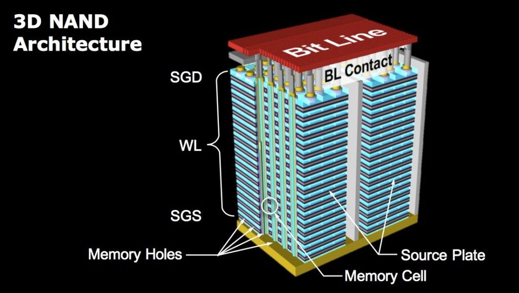
Moving to 3D to reduce cost per bit
The further increase in storage density is achieved by transitioning to the third dimension rather than stacking 2D layers like NAND, as the process steps required to do so would greatly increase the cost. The basic idea of true 3D NAND is to stack cells into vertical strings to achieve a higher density per unit area. In this configuration, cells are still addressed by horizontal lines.
The most common manufacturing method is the ring gate (GAA) vertical channel method, which starts with a growing oxide/nitride layer stack. Next, cylindrical holes are drilled down by stacking using advanced dry etching tools. A tunnel and trap layer is deposited along the lateral wall of the hole. To accomplish this punching and plugging process, a thin channel of polysilicon is deposited into the hole, followed by a core filling, forming a macaroni-like structure.
Next, remove the nitride and replace it with wire metal. In these GAA structures, the cylindrical gate wraparound channel structure enhances the ability of carrier injection into the capture layer, thus expanding the programming/erase window.
By adding more layers rather than shrinking feature sizes, the NAND flash industry has abandoned traditional scaling. The first commercial 3D NAND product was launched in 2013 with a stack count of 24-word line layers (128GB). The structure varies from vendor to vendor and is referred to as V-NAND and BICS.
As a result, 3D NAND is the first and only technology to bring true 3D products to market. In the following years, more layers were added on top of each other in order to maintain the trend of bit density. Recently, some major companies have introduced products based on 232-layer 3D NAND, and this trend of increasing layers is expected to continue in the coming years.
From floating grids to charge traps
Other innovations were adopted during the development process to facilitate challenging 3D processes or further increase bit density. For example, increase bit density: by up to 4 bits per cell, which is a real asset of NAND flash technology. In the case of 4 bits, a large enough storage window can activate multiple batteries, supporting up to 16 independent charge levels per transistor.
Another innovation is to replace the floating gate unit with a charge-trap unit, which means a simpler process. The two types of cells work in a relatively similar way, but in charge-capture cells, the trapping layer is an insulator, usually silicon nitride, which provides less electrostatic interference between adjacent cells. This charge trap unit is now the basis of most 3D NAND structures.
Improve bit storage density
In order to maintain the NAND flash roadmap, some major vendors have recently announced plans to increase the number of layers to at least 500. According to the trend line, this number will increase to 1,000 in ten years. Increasing the number of layers introduces higher processing complexity, challenges deposition and etching processes, and causes stress to build up within the layers. In response to the challenge, NAND flash manufacturers have recently begun to split the number of layers into at least two, and stack the individually processed layers on top of each other.
However, there are concerns that this evolution will gradually reduce the cost efficiency of NAND flash products without significant innovation. The increase in layers required investment in highly advanced deposition and corrosion tools. The trend of multi-layer stacking will greatly increase the number of masks, processing steps, and time. It could also lead to a slower storage roadmap, as the 1000-layer stack won’t be available until 2030.
As the number of layers increases, the pressure reduces layer thickness and controls stack height due to patterning and stress causes. This z-spacing scaling reduces the height of all materials in the stack, including word-line metals and oxides.
Z-spacing scaling
The scaling of the Z-spacing may be supplemented by a further reduction in the X-y dimensions. The evolution of 3D NAND requires significant innovation in storage units, and that hasn’t changed. Therefore, new materials and battery structures are being explored as alternatives to GAA NAND flash batteries.
Of interest during development are the grooves that connect the transistors. In this architecture, the storage unit is no longer circular. They are achieved on the sidewalls of the trench, with two transistors at either end of the trench increasing the bit density. From an operational point of view, grooved cells are similar to flat cell cells compared to round GAA NAND flash cells.
Although it has a few flaws in its electrical properties (such as program/erase Windows), the grooved structure can reduce the unit cell area in the X-y direction compared to “GAA” cells. As a result, grooved cells are proposed as the next-generation NAND flash battery architecture, which is expected to reduce the X-Y spacing from today’s 140nm to about 30nm.
END.
Recommended Reading:


